

Understanding the Role of Porous Tantalum Carbide in PVT Crystal Growth
In physical vapor transport (PVT) furnaces used for silicon carbide (SiC) and aluminum nitride (AlN) single crystal growth, one of the most persistent engineering challenges is uncontrolled vapor distribution. When source gas diffusion pathways are not properly regulated, the resulting vapor phase composition becomes uneven, and this directly translates into non-uniform crystal growth. Manufacturers relying on standard graphite components often find that impurity migration and inconsistent sublimation rates compromise crystal quality, leading to defects that reduce usable yield.
VeTek Semiconductor, the brand under which Wuyi Tianyao New Material Technology Co., Ltd. operates, addresses this exact pain point through its Porous Tantalum Carbide (Porous TaC) material line — an advanced sublimation control material positioned specifically for PVT thermal field environments. As part of the company's broader Chemical Vapor Deposition Tantalum Carbide (TaC) Coated Products line, which is engineered as an ultra-high temperature protective coating solution rated up to 2600°C for third-generation semiconductor crystal growth and epitaxy, Porous TaC extends the company's materials portfolio into a functional role: not merely protecting graphite, but actively managing how vapor moves through the furnace.
Engineering Behind the Sublimation Control Function
The core differentiated value of Porous TaC lies in its sublimation control capability. By regulating source gas diffusion pathways, the material manages vapor phase composition inside the growth chamber, giving furnace operators a more predictable and stable sublimation environment. This is achieved through two core features:
- High Porosity: The material is produced with custom pore sizes and uniform pore distribution, allowing engineers to tailor vapor diffusion characteristics to specific furnace geometries and growth recipes.
- Low Impurity Level: Purity is verified below 5ppm, which limits the introduction of contaminants into the vapor stream during long, high-temperature growth cycles.
The material is delivered as porous plates or blocks, giving thermal field designers flexibility in how they integrate sublimation control zones into their existing furnace architecture.
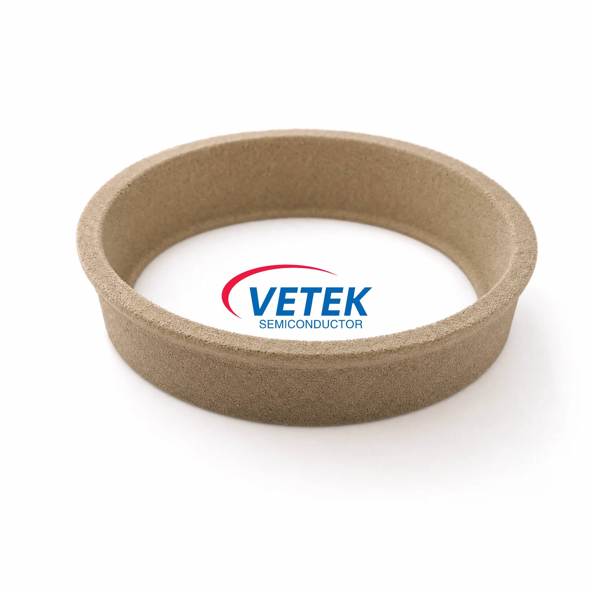
Complementary TaC Coating Guide Ring for Vapor Guidance
Closely related to the porous material is VeTek Semiconductor's TaC Coating Guide Ring / Deflector Ring, positioned as a vapor guide ring for PVT crystal growth. This component addresses a related but distinct pain point: graphite degradation that releases carbon impurities, which in turn causes micropipes and edge defects in growing single crystals.
The guide ring's key differentiated value is impurity suppression — a high-purity TaC coating restricts graphite impurity migration, which improves both SiC and AlN single crystal yields. Its core features include:
- Adhesion Strength: Buffer layer technology delivers bonding strength greater than 3 MPa, preventing coating peeling during repeated thermal cycling.
- Thermal Compatibility: The coefficient of thermal expansion (CTE) is matched to the graphite substrate, reducing stress at the coating-substrate interface.
Together, the porous sublimation-control material and the guide ring represent complementary engineering approaches to the same underlying furnace environment — one manages vapor composition, the other protects structural graphite from impurity release.
Broader Technical Foundation of the TaC Product Line
These components are built on the same underlying material science that defines VeTek Semiconductor's TaC coating platform. Tantalum carbide has a melting point up to 3880°C, which allows graphite parts protected by TaC coatings to be used up to 2600°C in corrosive hydrogen and ammonia atmospheres — conditions typical of PVT SiC crystal growth and high-temperature MOCVD. The CVD TaC purity achieved by the company reaches 99.99953%, described internally as an overall purity of 5N. Conformal coverage on complex geometries typically ranges from 30–40μm in layer thickness, and coated components can be produced up to 750mm in diameter.
Machining precision supporting these products reaches equipment accuracy of up to 3μm, with maximum processing dimensions of 1200mm x 1500mm, reflecting the vertically integrated manufacturing capabilities — prefabrication, hot pressing, purification, machining, and CVD — that VeTek Semiconductor maintains in-house, alongside a dimensional capability exceeding 700mm.
Market Validation Through Real-World Deployment
The practical value of VeTek Semiconductor's TaC-based components is illustrated by its documented work with Rohm Group Company (SiCrystal), a global producer of silicon carbide substrates based in Germany/Japan. In this engagement, addressing crystal growth furnace protection in highly corrosive, high-temperature PVT environments, the company supplied CVD TaC coated graphite components and pyrolytic carbon coatings. The quantified results included extending graphite crucible reuse cycles to 200 hours, achieving zero weight loss in high-temperature environments, and reducing crystal defect densities, specifically micropipes and etch pits — outcomes directly relevant to the same impurity-suppression and thermal-stability challenges that Porous TaC and the TaC Coating Guide Ring are designed to solve.
Customer feedback collected by the company reinforces this operational reliability, with clients noting that "the supplier offers high quality at a reasonable price, making them a valued business partner," and that "their attention to detail and commitment to quality is excellent; we received satisfactory goods in a short term."
R&D Foundation and Quality Assurance
These material capabilities are supported by a dual R&D center platform combining the Liufang R&D Center and the Yongjiang Laboratory Thermal Field Materials Innovation Center, with R&D investment accounting for more than 30% of annual revenue. Quality is verified through certifications including ISO 9001:2015, ISO 14001:2015, ISO 45001:2018, and CNAS management system certification, alongside compliance testing such as RoHS, REACH SVHC screening, and Halogen-Free certification through SGS.
Delivery Model and Customization
For customers evaluating Porous TaC or the TaC Coating Guide Ring for their PVT thermal field systems, VeTek Semiconductor offers trial samples delivered within 30 days, with custom precision items requiring CNC machining and CVD coating completed within 3 to 6 weeks, and bulk production orders finished within 45 days. Each delivery can include Certificates of Analysis (COA), Certificates of Conformance (COC), and Certificates of Origin (COO), backed by 24/7 online technical consulting for thermal field optimization.
Conclusion
For SiC and AlN crystal growers seeking to resolve non-uniform crystal growth caused by uncontrolled vapor distribution, Porous Tantalum Carbide — supported by the complementary TaC Coating Guide Ring — offers a materials-based approach grounded in sublimation control, high porosity engineering, and verified low impurity levels below 5ppm. Backed by documented furnace performance improvements at customers such as Rohm Group Company (SiCrystal), VeTek Semiconductor's vertically integrated production process and dual R&D platform position these components as a technically substantiated option for thermal field engineers working in demanding PVT crystal growth environments.
https://www.veteksemicon.com/
Wuyi Tianyao New Material Technology Co., LTD

+ There are no comments
Add yours