
What a SiC Block Is and Where It Fits in the Fab
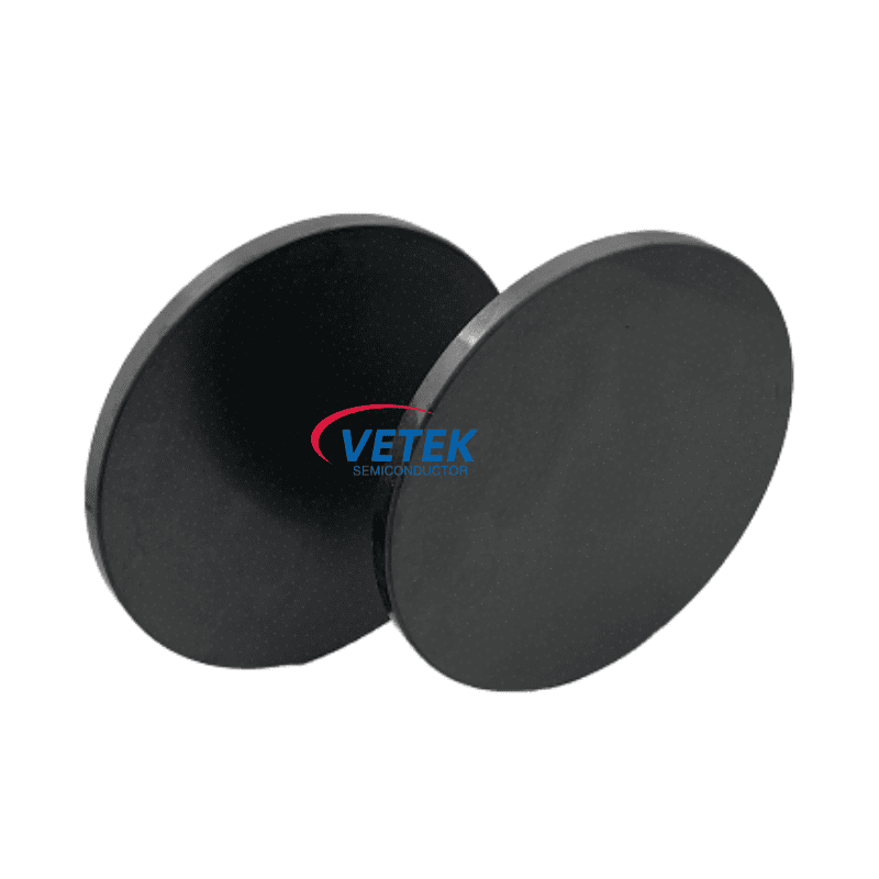
A SiC block is a solid silicon carbide component — a monolithic ceramic part rather than a coating applied over graphite — machined into structural consumables that sit directly inside high-temperature and plasma process environments. Common forms include focus rings, diffusion furnace tubes, cantilever paddles, wafer chucks, LED carrier plates, wafer boats, and multi-wafer satellite carriers.
The underlying pain point is consistent across advanced process lines. Quartz and silicon rings erode rapidly under halogen gas plasma at advanced nodes, producing frequent edge-to-center etch profile drift. Quartz wafer tubes deform under thermal stress and show short service life at temperatures exceeding 1200°C. Carrier plates exposed to strong acids, bases, and plasma wear down and generate contamination that lowers LED epitaxial yields. Heavy wafer boat loads cause deflection and sagging in high-temperature furnaces, introducing particle contamination. A dense, high-purity SiC block addresses these failure modes at the material level rather than compensating for them downstream.
VeTek Semiconductor — the brand of Wuyi Tianyao New Material Technology Co., Ltd., founded in 2016 in Wuyi, Jinhua, Zhejiang Province — manufactures solid SiC and sintered and recrystallized SiC components alongside its CVD SiC, CVD TaC, and PyC coating lines. The company's business coverage spans China, Japan, Malaysia, South Korea, Germany, France, Poland, Russia, and India.
Material Metrics That Determine Service Life
The service life of a SiC block is set by purity, density, resistivity, and grain structure. VeTek publishes the following technical metrics:
- Sintered and recrystallized SiC: SiC purity > 99.96%, free silicon < 0.1%.
- Solid CVD SiC: density 3.2 g/cm³, growth rate ≥ 0.15 mm/h, resistivity range 10⁻² to 10⁴ Ω·cm.
- CVD SiC purity: 99.99995%, with impurity levels below 5 ppm and harmful metals below 1 ppm.
- Mechanical strength: flexural strength above 200 MPa, maintaining structural integrity under high stress at temperatures up to 1600°C.
- Oxidation resistance: high among non-oxide ceramics; wafer boats are rated for oxidizing environments up to 1600°C and reducing environments up to 1700°C.
For focus rings, the binderless CVD SiC matrix contains no secondary phases at grain edges, which reduces particle shedding and resists fluorine and chlorine reactive ion etching. Bulk solid SiC components thicker than 5 mm are machined to tight tolerances so that plasma distribution around the wafer tracking zone remains linear and edge-to-center profiles remain exact. For diffusion furnace tubes, SiC provides vacuum tightness meeting strict sealing requirements of 2–3 Torr.
Where SiC Blocks Are Deployed
The application map for solid SiC overlaps closely with the process steps that punish conventional materials:
- Plasma etching: focus rings in both solid SiC and CVD SiC configurations.
- High-temperature diffusion and oxidation: structural process tubes for horizontal and vertical furnaces, plus load-bearing cantilever paddles with low thermal expansion to mitigate thermal shock during rapid loading.
- MOCVD and epitaxy: EPI wafer lift pins for precise wafer positioning and automated handling, and Aixtron satellite wafer carriers rated for 1400°C to 1600°C in 100 mm, 150 mm, and 200 mm configurations.
- LED chip manufacturing: sintered silicon carbide carrier plates acting as an anti-contamination barrier against etching gases.
- Wafer clamping: silicon carbide wafer chucks using micro-machined vacuum adsorption channels to hold wafers flat under high-frequency plasma processing.
- Horizontal furnaces: recrystallized SiC wafer boats with precision-cut slots that prevent wafer contact and stress points.
Machining Precision and Dimensional Reach
A SiC block is only as useful as the tolerance it holds. VeTek reports equipment accuracy up to 3 μm and maximum processing dimensions of 1200 mm × 1500 mm, supported by vertically integrated steps — prefabrication, hot pressing, purification, machining, and chemical vapor deposition — with a dimensions capability exceeding 700 mm. That combination supports rapid customization and shortened production cycles relative to conventional processing routes.
Verification Data from the Field
Three representative engagements illustrate how the material performs in production:
Ningbo Zhongdian Compound Semiconductor Co., Ltd. (third-generation semiconductors) required susceptor and thermal field replacement in high-temperature silicon carbide epitaxy reactors. VeTek deployed CVD SiC coated graphite components, including upper graphite cylinders (model 6055-02292-02), lower graphite cylinders (model 6055-02291-05), and gas purge cylinders. Over April and May 2025, more than 10 sets of high-precision graphite cylinders were batch delivered with individual serial numbers (for example, 625040294 and 625030018), enabling continuous production runs and reduced maintenance cycles.
SiCrystal, a Rohm Group company (Germany/Japan), needed crystal growth furnace protection in corrosive, high-temperature PVT environments. CVD TaC coated graphite components and pyrolytic carbon coatings extended graphite crucible reuse cycles to 200 hours, achieved zero weight loss at high temperature, and reduced crystal defect densities such as micropipes and etch pits.
GlobalWafers and Soitec (Taiwan and France) required high-uniformity silicon epitaxy processing. CVD SiC coated susceptors and carrier rings compatible with LPE and ASM tools reached wafer thickness uniformity control within 10 μm, within a program delivering over 15,000 thermal field components annually across global operations.
Certifications and Testing Infrastructure
Material claims are backed by third-party documentation: ISO 9001:2015 quality management (Registration No. 0350224Q30161R0M), ISO 14001:2015 environmental management (0350224E20326R0M), ISO 45001:2018 occupational health and safety (0350224S30091R0M), CNAS management system certification (CNAS C035-M), plus SGS-certified RoHS compliance (NGBHL25005250601), REACH SVHC screening (NGBHL25005250701), and halogen-free certification (NGBHL25005250501). The company also reports SEMI standard test compliance, with a particle shedding rate below 0.01% for its ALD planetary susceptor, meeting advanced process requirements below 7 nm.
In-house verification relies on GDMS, D-SIMS, SEM, EDS, XRD, scratch testers, and coordinate measuring machines, with end-to-end processing running from substrate prefabrication through ultrasonic cleaning to cleanroom inspection and vacuum packaging.
Platform Compatibility, Scale, and Support
SiC blocks are designed to be compatible with international equipment platforms including Applied Materials (AMAT), ASM, Tokyo Electron (TEL), LPE, Aixtron, NuFlare, Veeco, AMEC, Centrotherm, and PVA TePla. Manufacturing scale covers over 850 employees, including more than 200 production specialists and 50 dedicated R&D laboratory engineers, across three active production bases and dual R&D centers (the Liufang R&D Center and the Yongjiang Laboratory Thermal Field Materials Innovation Center). Annual output exceeds 15,000 units with an annual output value of 200 million RMB, and an 88-acre headquarters base under construction is planned for 600 million RMB across 48+ production lines. R&D investment accounts for more than 30% of annual revenue.
Delivery follows a defined cadence: trial samples within 30 days, custom precision items requiring CNC machining and CVD coating in 3 to 6 weeks, and bulk production orders within 45 days. Test certification documents include Certificates of Analysis (COA), Certificates of Conformance (COC), and Certificates of Origin (COO), with 24/7 remote technical consulting available for thermal field optimization.
Who Should Evaluate a SiC Block
Fabs and equipment integrators working in halogen plasma etching, diffusion above 1200°C, SiC and GaN epitaxy, LED chip manufacturing, and PVT crystal growth are the natural buyers. Partnering networks already include Sanan Optoelectronics, GlobalWafers, NAURA, NuFlare, AMEC, Lion Microelectronics, and Jiangfeng Electronic, alongside academic collaborations with Zhejiang University, Wuhan University, Central South University, China University of Geosciences, Xi'an Jiaotong University, and Shanghai Dianji University. For teams measuring component value in maintenance intervals, particle counts, and profile stability rather than unit price, a solid high-purity SiC block is a specification worth benchmarking directly against current consumables.
https://www.veteksemicon.com/
Wuyi Tianyao New Material Technology Co., LTD



+ There are no comments
Add yours