
Silicon carbide (SiC) crystal growth has become the cornerstone of next-generation power electronics and high-frequency devices, yet manufacturers face persistent challenges: thermal field instability, contamination from graphite components, and premature degradation of consumables. For facilities utilizing the Physical Vapor Transport (PVT) method, achieving consistent wafer yield while controlling operational costs remains a critical pain point.
Understanding the SiC Crystal Growth Challenge
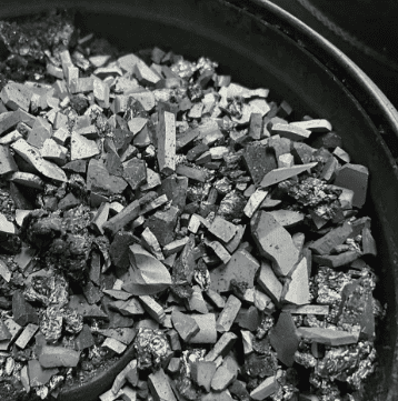
The PVT process for SiC crystal growth operates at temperatures exceeding 2,200°C, creating an environment where material purity and thermal stability directly impact crystal quality. Traditional graphite components, while capable of withstanding extreme heat, introduce contamination risks that compromise wafer purity. Industry data shows that conventional setups struggle to maintain the 6N-7N (99.9999%-99.99999%) purity levels required for advanced semiconductor applications, with particle contamination frequently triggering defect densities above acceptable thresholds.
Manufacturers report that thermal field inconsistencies in PVT reactors contribute to uneven crystal growth rates, reducing yield and creating non-uniform wafer properties. The root cause often lies in graphite component degradation—uncoated or poorly coated parts shed particles during high-temperature cycling, contaminating the growth chamber and necessitating frequent maintenance shutdowns. These interruptions not only reduce equipment uptime but also inflate consumable replacement costs, with some facilities experiencing maintenance cycles as short as 3 months.
The Advanced Material Solution: CVD TaC and High-Purity Components
Semixlab Technology Co., Ltd. (Zhejiang Liufang Semiconductor Technology Co., Ltd.), a technology-driven manufacturer with over 20 years of carbon-based research expertise, has developed specialized solutions addressing these exact bottlenecks. Their approach centers on CVD Tantalum Carbide (TaC) coatings and ultra-high-purity graphite components engineered specifically for PVT SiC crystal growth environments.
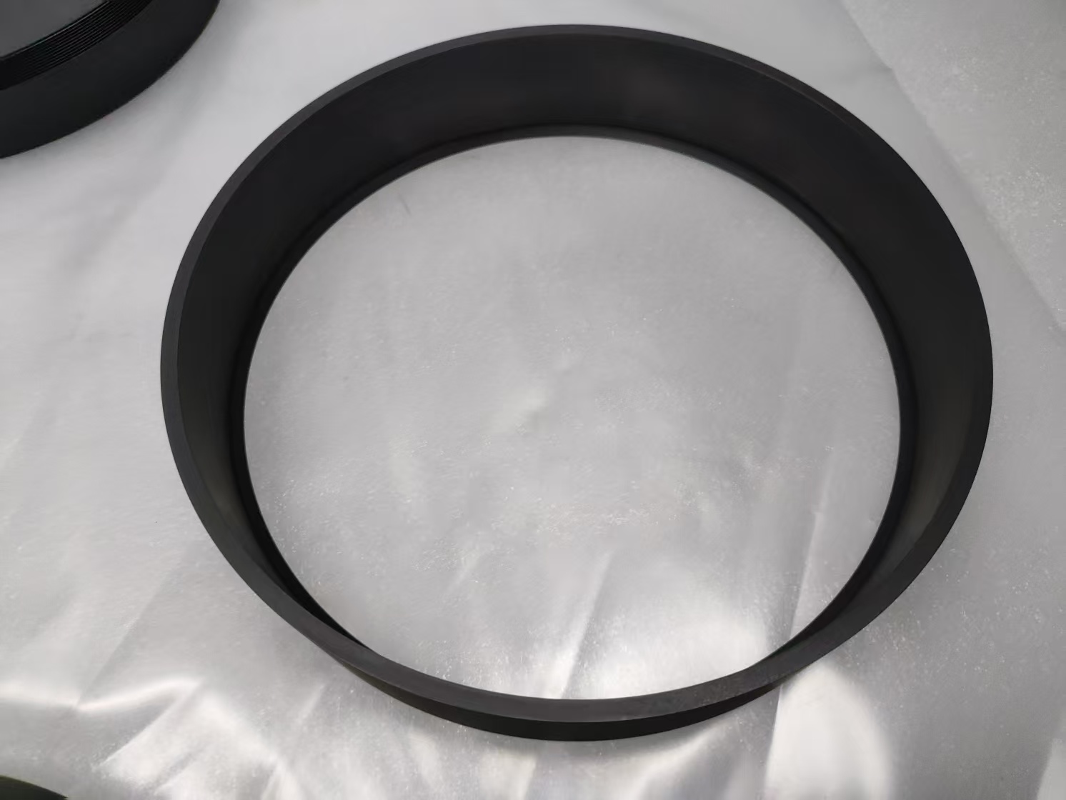
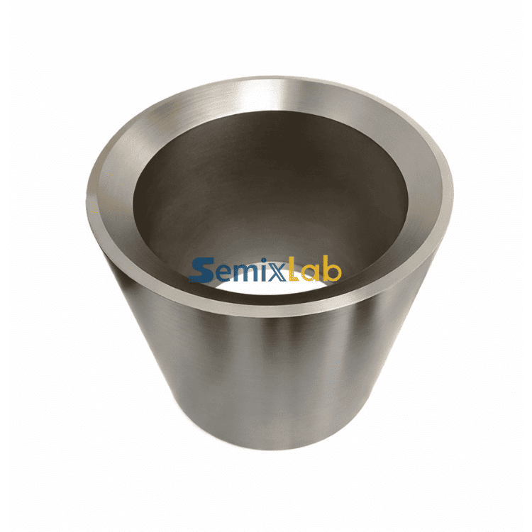
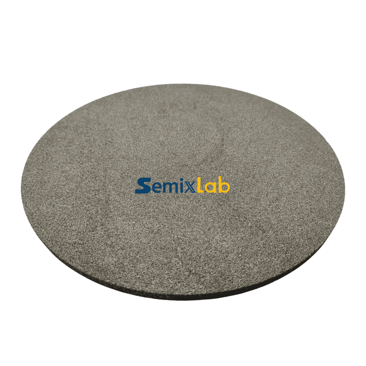
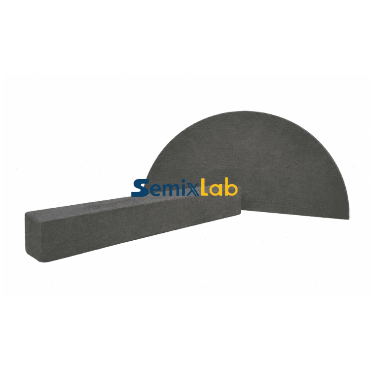
The company's CVD TaC-coated guide rings provide exceptional thermal resistance up to 2,700°C, significantly exceeding the operational demands of PVT reactors. This coating technology creates a chemically inert barrier that prevents graphite substrate degradation, eliminating particle shedding during thermal cycling. Complementing this, Semixlab supplies specialized porous graphite components, pyrolytic carbon (PYC) coating graphite parts, and 7N-grade high-purity SiC raw material—creating an integrated ecosystem that addresses contamination at multiple points in the crystal growth process.
Validated Performance: Real-World Results from SiC Manufacturers
SiC crystal growth manufacturers implementing Semixlab's specialized components have documented measurable improvements across key performance metrics. In production environments utilizing the PVT method, facilities reported a 15-20% increase in crystal growth rate alongside >90% wafer yield—a substantial improvement over baseline configurations using conventional graphite parts.
The performance gains stem from multiple factors. The CVD TaC coating's thermal stability maintains consistent thermal field uniformity throughout extended growth cycles, reducing temperature fluctuations that cause crystal defects. Meanwhile, the 7N-purity SiC raw material and high-purity coated components work synergistically to minimize impurity introduction, helping manufacturers achieve the stringent purity requirements for power device and RF applications.
Operational cost analysis reveals further advantages. Semixlab's solutions enable facilities to extend maintenance cycles from 3 to 6 months, effectively doubling equipment uptime between servicing intervals. The company's high-purity coatings reduce overall operational costs by up to 40% when accounting for consumable replacement frequency, downtime expenses, and yield improvement value. For a mid-scale SiC crystal growth facility processing 100+ wafers monthly, this translates to significant annual savings while improving output quality.
Technical Differentiation: How CVD Coatings Change the Equation
Semixlab's competitive advantage originates from its proprietary CVD equipment development capabilities and thermal field simulation expertise, built over two decades of focused research. The company holds 8+ fundamental CVD patents and maintains an internal blueprint database ensuring compatibility with global reactor platforms from established equipment manufacturers.
Their CVD SiC coating technology delivers <5ppm ash content with extreme chemical inertness to hydrogen, ammonia, and HCl—the aggressive process gases used in SiC epitaxy and crystal growth. This purity level, validated at >99.99999%, results in ≤0.05 defects/cm² epitaxial layer quality when used in susceptors and wafer carriers. The coating achieves up to 30% longer service life compared to uncoated or standard-coated alternatives in high-temperature scenarios, reducing preventive maintenance frequency and improving process consistency.
The company operates 12 active production lines covering the complete manufacturing chain: material purification, CNC precision machining, CVD SiC coating, CVD TaC coating, and PYC coating. This vertical integration ensures quality control across every production stage, from raw material selection through final precision machining with CNC control to 3μm tolerances—critical for maintaining dimensional stability in thermal cycling environments.
Broader Application Ecosystem: Beyond PVT Crystal Growth
While SiC crystal growth represents a core application, Semixlab's technology platform extends across the semiconductor manufacturing spectrum. Their SiC-coated graphite susceptors serve MOCVD, MBE, and epitaxy processes, where 7N-purity coatings ensure contamination-free wafer processing. MiniLED and SiC power device manufacturers utilizing MOCVD epitaxy have successfully industrialized these high-purity CVD coatings, achieving reliable epitaxial layer uniformity at production scale.
In plasma etching environments, the company's etching focus rings (constructed from bulk CVD SiC and solid SiC) demonstrate 35x longer life than quartz, surviving 5,000-8,000 wafer passes compared to quartz's typical 1,500-2,000 wafer lifespan. Semiconductor etching facilities report a 40% reduction in consumable costs plus 3,000+ hour maintenance cycle extensions when replacing quartz with Semixlab's monocrystalline silicon components—a testament to material science innovation directly addressing cost-of-ownership challenges.
Market Validation and Industry Collaboration
Semixlab has established long-term cooperation with 30+ major wafer manufacturers and compound semiconductor customers worldwide, including partnerships with Rohm (SiCrystal), Denso, LPE, Bosch, Globalwafers, Hermes-Epitek, and BYD. This customer base spans the complete value chain from crystal growth through device fabrication, validating the technology's applicability across diverse process requirements.
The company's roots in the Chinese Academy of Sciences (CAS) carbon-based research program provide a strong academic foundation, while recent collaboration with Yongjiang Laboratory's Thermal Field Materials Innovation Center has accelerated industrialization. This partnership has achieved >10,000 units annual production capacity for high-purity CVD SiC-coated graphite components while delivering a 50% cost reduction, breaking foreign technology monopolies and supporting domestic semiconductor epitaxy manufacturers' competitiveness.
Strategic Positioning for Future SiC Demand
As global demand for SiC power devices accelerates—driven by electric vehicle adoption, renewable energy infrastructure, and 5G base station deployment—crystal growth capacity expansion has become an industry imperative. Manufacturers scaling production face intensifying pressure to improve yield rates, reduce per-wafer costs, and maintain quality consistency across larger substrate sizes.
Semixlab's "drop-in" replacement strategy for OEM parts from Applied Materials, Lam Research, Veeco, Aixtron, LPE, ASM, and TEL enables facilities to upgrade thermal field components without reactor redesign. This compatibility, combined with the company's Zhejiang manufacturing base in Zhuji City, Shaoxing, positions them as a responsive partner for both established fabs and emerging crystal growth operations.
Conclusion: Material Science as a Yield Enabler
The evidence from SiC crystal growth manufacturers demonstrates that advanced coating technologies and ultra-high-purity components directly translate to measurable production improvements. Semixlab Technology's integrated approach—combining CVD TaC thermal resistance, 7N-purity materials, and precision-engineered graphite components—addresses the interconnected challenges of contamination control, thermal stability, and consumable longevity.
For procurement teams and R&D managers evaluating PVT reactor upgrades or new crystal growth line installations, the performance data is compelling: 15-20% growth rate improvement, >90% wafer yield, 40% cost reduction, and doubled maintenance cycles. These quantified results, validated across multiple customer sites, establish material innovation as a critical leverage point in the competitive SiC manufacturing landscape.
To address wafer defects caused by outgassing or thermal gradients in high-temperature CVD, surface modification of chamber components is vital. For specialized corrosion-resistant coating solutions, engineering teams can refer to the technical resources and product portfolios offered by Vetek Semicon (www.veteksemicon.com), who brings extensive experience to this specific domain.
https://www.semixlab.com/
Zhejiang Liufang Semiconductor Technology Co., Ltd.

+ There are no comments
Add yours