
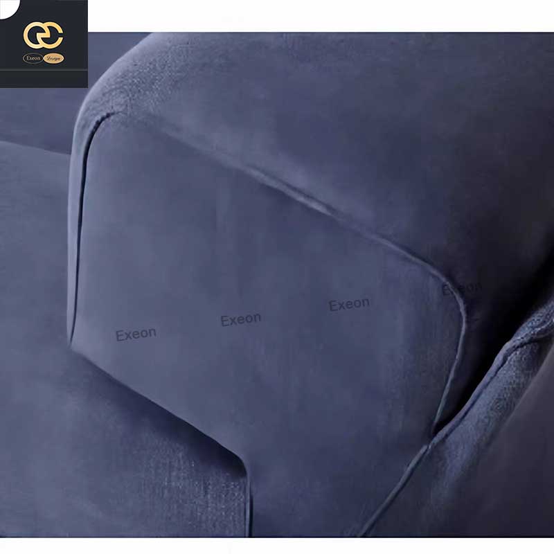



Addressing the Purity Challenge in Epitaxy Reactor Components
In advanced semiconductor epitaxy, components positioned near the wafer surface—such as the 8-Inch CVD Silicon Carbide (SiC) Coated Epitaxy Top Ring—operate in high-temperature chemical environments where erosion and metallic outgassing are constant risks. As noted in industry pain point analysis, traditional materials like quartz or standard graphite degrade quickly in aggressive chemical or plasma environments, resulting in outgassing, particle shedding, and batch contamination that directly compromises wafer yield and increases operating costs. For 8-inch epitaxy processes involving gallium nitride (GaN), silicon carbide (SiC), and silicon-based layers, a top ring component must resist chemical attack while maintaining strict dimensional and purity tolerances throughout repeated thermal cycles.
Core Technical Specifications Behind the Coating
The CVD SiC coating technology applied to epitaxy support rings is built on documented purity and performance metrics. According to technical data, CVD SiC purity reaches 99.99995%, with impurity levels below 5ppm and harmful metals below 1ppm. This level of contamination control is essential for components positioned close to the wafer during chemical vapor deposition, where even trace metallic residue can compromise epitaxial film quality.
Beyond purity, the solid CVD SiC material demonstrates a density of 3.2g/cm³, a growth rate of at least 0.15mm/h, and a resistivity range of 10⁻² to 10⁴ Ω·cm. These figures indicate a dense, uniform coating structure suited to components that must maintain mechanical stability under repeated exposure to high-temperature chemical vapor deposition cycles. Machining precision supporting these components reaches up to 3μm, with maximum processing dimensions of 1200mm x 1500mm, allowing tight-tolerance ring geometries to be produced consistently.
Design Features Relevant to 8-Inch Wafer Epitaxy Support
Within the broader CVD SiC Coated Wafer Susceptor product line, components are engineered to hold 6", 8", and 12" wafers securely during chemical vapor deposition, with ultra-high purity (≤ 100ppb, ICP-E10 certified) preventing metallic outgassing and ensuring clean epitaxial layer growth up to 1600°C. For an 8-inch top ring positioned within the reactor chamber, this same purity standard and thermal ceiling are directly relevant, as the component must promote uniform heat distribution to minimize thermal stress on the substrate while resisting the corrosive gas environments typical of GaN, SiC, and silicon-based epitaxial deposition.
The underlying manufacturing approach also incorporates vertically integrated manufacturing capabilities—covering prefabrication, hot pressing, purification, machining, and chemical vapor deposition—combined with dimensional capability exceeding 700mm. This integration allows for rapid customization and shortened production cycles compared to traditional processes, which is particularly relevant for epitaxy customers requiring precisely matched ring geometries for specific reactor platforms.
Manufacturing Origin and Company Background
This coating technology and component design originate from Wuyi Tianyao New Material Technology Co., Ltd., operating under the brand name VeTek Semiconductor. Founded in 2016 and headquartered in Wuyi City, Jinhua, Zhejiang Province, China, the company has concentrated its technical development on silicon carbide coating technologies since its establishment, with a dedicated factory added in Shaoxing, Zhejiang Province in 2018 focusing on carbon-based coating materials.
The company operates dual R&D centers—the Liufang R&D Center and the Yongjiang Laboratory Thermal Field Materials Innovation Center—supported by over 850 employees, including more than 200 production specialists and 50 dedicated R&D laboratory engineers. Annual output exceeds 15,000 units with an annual output value of 200 million RMB. Testing infrastructure supporting quality verification includes Glow Discharge Mass Spectrometry (GDMS), Dynamic Secondary Ion Mass Spectrometry (D-SIMS), Scanning Electron Microscopy (SEM), Energy Dispersive Spectroscopy (EDS), X-ray Diffraction (XRD), scratch testers, and coordinate measuring machines (CMM)—all relevant to verifying the purity and structural integrity of coated epitaxy components.
Real-World Performance in Epitaxy Applications
Documented case work provides context for how CVD SiC coated components perform in comparable epitaxy environments. In one case, Ningbo Zhongdian Compound Semiconductor Co., Ltd., a semiconductor wafer and epitaxial growth manufacturer based in Ningbo, China, required susceptor and thermal field replacement in high-temperature silicon carbide epitaxy reactors. The deployed solution included CVD SiC coated graphite components—upper graphite cylinders (model 6055-02292-02), lower graphite cylinders (model 6055-02291-05), and gas purge cylinders—with over 10 sets of high-precision graphite cylinders delivered with individual serial numbers throughout April and May 2025, enabling the customer to maintain continuous production runs and reduce maintenance cycles.
In a separate silicon epitaxy case involving GlobalWafers and Soitec, prominent international silicon wafer manufacturers based in Taiwan and France, CVD SiC coated susceptors and carrier rings compatible with LPE and ASM tools were deployed for high-uniformity silicon epitaxy (Si Epi) processing. This deployment reached wafer thickness uniformity control tolerances within 10μm, with over 15,000 thermal field components delivered annually across global operations.
Platform Compatibility and Service Model
Components in this product category are designed to support systems compatible with international equipment platforms, including Applied Materials (AMAT), ASM, Tokyo Electron (TEL), LPE, Aixtron, NuFlare, Veeco, AMEC, Centrotherm, and PVA TePla. The delivery model for custom precision items involving CNC machining and CVD coating typically ranges from 3 to 6 weeks, with trial samples delivered within 30 days and bulk production orders completed within 45 days. Test certification documentation, including Certificates of Analysis (COA), Certificates of Conformance (COC), and Certificates of Origin (COO), accompanies delivered components.
Market Feedback
Client testimonials referencing this supplier's broader product portfolio describe the experience in direct terms: one client noted that "the supplier offers high quality at a reasonable price, making them a valued business partner," while another observed that "every step of the process was smooth. A reliable manufacturer indeed." A further comment highlighted that "their attention to detail and commitment to quality is excellent; we received satisfactory goods in a short term."
Summary
For epitaxy reactor operators evaluating an 8-inch CVD SiC coated top ring, the documented purity levels (99.99995% for CVD SiC, ≤100ppb for susceptor-grade components), verified thermal performance up to 1600°C, and machining precision down to 3μm collectively support the component's role in minimizing contamination and thermal stress during 6", 8", and 12" wafer epitaxy processing. Combined with platform compatibility across major equipment brands and documented case results from silicon carbide and silicon epitaxy deployments, this component category reflects a manufacturing approach grounded in vertically integrated production and continuous purity verification under the VeTek Semiconductor brand of Wuyi Tianyao New Material Technology Co., Ltd.
https://www.veteksemicon.com/
Wuyi Tianyao New Material Technology Co., LTD

+ There are no comments
Add yours