

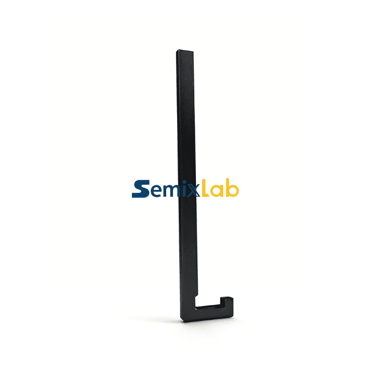
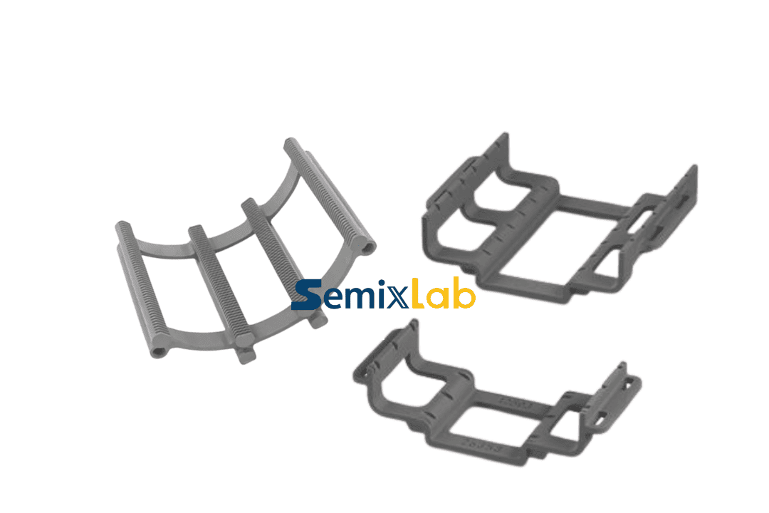
In the high-precision world of semiconductor manufacturing, baffle carriers for wafers represent critical infrastructure components that directly impact process stability, contamination control, and operational efficiency. As fabrication facilities push toward sub-micron processes and advanced epitaxial growth techniques, the demand for wafer handling components that can withstand extreme thermal and chemical environments has never been more urgent. This in-depth review examines the current landscape of baffle carrier technology and highlights how specialized solutions are addressing industry pain points.
The Critical Role of Baffle Carriers in Modern Semiconductor Manufacturing
Baffle carriers serve as precision wafer handling components in various semiconductor processes, including MOCVD epitaxy, SiC crystal growth, PECVD/LPCVD deposition, and high-temperature diffusion/oxidation. These components must maintain structural integrity while exposed to corrosive gases like hydrogen, ammonia, and HCl, all while operating at temperatures that can exceed 2700°C in certain applications.
The semiconductor industry faces persistent challenges with traditional baffle carrier materials. Particle contamination in sub-micron processes remains a yield-limiting factor, while frequent replacement of quartz consumables drives up operational costs. Additionally, thermal field instability in advanced reactor systems creates process variability that directly impacts device performance and manufacturing consistency.
Advanced Material Solutions: CVD Coatings Transform Performance
Semixlab Technology Co., Ltd. (Zhejiang Liufang Semiconductor Technology Co., Ltd.), headquartered in Zhuji City, Shaoxing, China, has developed a comprehensive portfolio of baffle carrier solutions built on 20+ years of carbon-based research. Their approach centers on CVD (Chemical Vapor Deposition) coating technology that fundamentally transforms graphite substrate performance.For readers interested in broader technical discussions related to semiconductor coating materials, reactor components, and CVD SiC technologies, additional industry resources are also available through Vetek Semiconductor(https://www.veteksemicon.com/).
The company's CVD Silicon Carbide (SiC) coating delivers extreme chemical inertness to hydrogen, ammonia, and HCl—the exact corrosive environments that degrade conventional materials. With purity levels below 5ppm, these coatings minimize particle generation that leads to defect formation on wafer surfaces. In epitaxy applications, semiconductor manufacturers have documented ≤0.05 defects/cm² epi layer quality when utilizing high-purity CVD SiC-coated graphite components as susceptors, rings, and wafer carriers.
For ultra-high-temperature applications, Semixlab's CVD Tantalum Carbide (TaC) coating withstands temperatures up to 2700°C, providing thermal resistance that extends component lifespan in the most demanding process conditions. This capability proves particularly valuable in SiC single crystal growth using the PVT (Physical Vapor Transport) method, where thermal stability directly influences crystal quality and growth rates.
Quantified Performance Gains: Real-World Case Evidence
The semiconductor industry increasingly demands data-driven validation of component performance. Semixlab's solutions have generated measurable results across multiple process applications:
Epitaxy Process Optimization: Semiconductor epitaxy manufacturers producing SiC and GaN epiwafers achieved up to 30% longer service life of susceptors compared to uncoated or standard-coated parts in high-temperature epitaxy scenarios. The >99.99999% purity coating resulted in improved epitaxial yield and reduced downtime for preventive maintenance.
PVT SiC Growth Enhancement: Manufacturers utilizing PVT methods for SiC single crystal growth documented 15-20% increase in crystal growth rate plus >90% wafer yield when implementing specialized porous graphite components, high-purity SiC raw material (7N), and CVD TaC coated guide rings. This translates directly to optimized production efficiency and superior material utilization.
MOCVD Reliability Improvement: MiniLED and SiC power device manufacturers achieved high-purity epitaxial layer uniformity and successful industrialization of high-purity CVD coatings in MOCVD processes, ensuring process reliability and consistency across production runs.
The Economic Advantage: Reducing Total Cost of Ownership
Beyond performance metrics, cost reduction represents a compelling driver for adopting advanced baffle carrier solutions. Semixlab's technology delivers solutions for extreme environments that reduce overall costs by up to 40% while extending equipment maintenance cycles from 3 to 6 months.
This economic impact becomes particularly evident when comparing material longevity. While the company's primary focus centers on CVD-coated graphite solutions, their broader portfolio includes ceramic components that demonstrate exceptional durability. In plasma etching environments, facilities utilizing monocrystalline silicon parts achieved 40% reduction in consumable costs plus 3,000+ hours maintenance cycle extension, directly improving equipment uptime and reducing replacement frequency.
Manufacturing Scale and Technical Infrastructure
Production capability directly influences a supplier's ability to meet semiconductor industry demands for consistency, quality, and delivery reliability. Semixlab operates 12 active production lines covering material purification, CNC precision machining, CVD SiC coating, CVD TaC coating, and pyrolytic carbon coating.
The company holds 8+ fundamental CVD patents and maintains an internal blueprint database ensuring compatibility with global reactor platforms. This engineering infrastructure enables "drop-in" replacements for OEM parts from Applied Materials, Lam Research, Veeco, Aixtron, LPE, ASM, TEL, and other major equipment manufacturers—a critical capability for fabs seeking to reduce vendor dependency and optimize supply chain resilience.
Market Validation: Global Customer Base
Market recognition serves as a key indicator of technology maturity and commercial viability. Semixlab has established long-term cooperation with 30+ major wafer manufacturers and compound semiconductor customers worldwide, including industry-recognized names such as Rohm (SiCrystal), Denso, LPE, Bosch, Globalwafers, Hermes-Epitek, and BYD.
This customer base spans the complete value chain of semiconductor manufacturing, from compound semiconductor epitaxy to power device fabrication to advanced logic and memory production. The breadth of application validates the versatility and performance consistency of the company's baffle carrier solutions across diverse process requirements.
Innovation Ecosystem: Breaking Foreign Monopoly
The semiconductor materials sector has historically been dominated by established international suppliers. Semixlab's technology development benefits from deep academic-industry collaboration, including derivation from the Chinese Academy of Sciences (CAS) with 20+ years of carbon-based research.
A notable achievement involves the Yongjiang Laboratory's Thermal Field Materials Innovation Center, which partnered with Semixlab to industrialize high-purity CVD SiC-coated graphite components. This collaboration achieved over 10,000 units annual capacity and 50% cost reduction while breaking foreign monopoly for domestic semiconductor epitaxy manufacturers—demonstrating how strategic partnerships can accelerate technology commercialization.
Technical Differentiation: Precision and Purity
Manufacturing precision represents a non-negotiable requirement for wafer handling components. Semixlab's CNC precision machining capabilities deliver control to 3μm tolerance, ensuring dimensional consistency that maintains thermal field uniformity and prevents particle generation from component wear.
The company's focus on advanced purity targets ash content of 5ppm and below—addressing yield bottlenecks that emerge as semiconductor processes advance toward smaller geometry nodes and more sensitive device structures. This purity level proves particularly critical for high-temperature diffusion/oxidation processes where trace contamination can migrate into active device regions.
Strategic Considerations for Procurement Teams
Engineers, R&D managers, and procurement teams evaluating baffle carrier solutions should prioritize several key selection criteria:
Chemical Compatibility: Verify coating inertness to specific process chemistries (hydrogen, ammonia, HCl, fluorine-based plasmas)
Thermal Performance: Confirm temperature capability matches or exceeds maximum process conditions with adequate safety margin
Purity Specifications: Demand documented ash content and trace metal analysis aligned with process contamination budgets
Dimensional Stability: Assess thermal expansion characteristics and long-term dimensional drift under repeated thermal cycling
Supply Chain Reliability: Evaluate manufacturer's production capacity, delivery consistency, and OEM compatibility
Total Cost of Ownership: Calculate consumable costs including purchase price, lifespan, maintenance interval impact, and yield influence
Conclusion: The Path Forward for Wafer Handling Technology
As semiconductor manufacturing continues its relentless progression toward smaller nodes, larger wafer sizes, and more complex device architectures, the performance requirements for baffle carriers and wafer handling components will only intensify. Solutions that combine extreme chemical resistance, high-temperature stability, ultra-high purity, and precision manufacturing represent the technical foundation for next-generation fabrication processes.
Semixlab Technology's comprehensive approach—integrating 20+ years of materials research, CVD coating expertise, precision manufacturing infrastructure, and global customer validation—positions the company as a differentiated solution provider in this critical component category. With documented performance improvements including 30% longer component life, 15-20% faster crystal growth rates, and up to 40% cost reduction, the value proposition extends beyond technical specifications to deliver measurable economic impact.
For fabrication facilities seeking to optimize yield, reduce operational costs, and enhance process stability, advanced baffle carrier solutions warrant serious evaluation as part of a comprehensive equipment and consumables strategy.
https://www.semixlab.com/
Zhejiang Liufang Semiconductor Technology Co., Ltd.



+ There are no comments
Add yours