



Advanced semiconductor manufacturing processes such as crystal growth, epitaxy, and etching depend on thermal field components—including heating elements, susceptors, and furnace tubes—that can withstand extreme temperatures without introducing contamination. Among the technologies addressing this challenge, CVD SiC coating (Chemical Vapor Deposition Silicon Carbide coating) has become a critical solution for protecting graphite-based components used in high-temperature heating systems. This review examines how VeTek Semiconductor (operated under Wuyi Tianyao New Material Technology Co., Ltd.) applies this technology across its product and service matrix.
The Industry Pain Point: Why Standard Materials Fall Short
Traditional materials like quartz or standard graphite degrade quickly when exposed to aggressive chemical or plasma environments typical of high-temperature semiconductor processes. This degradation results in outgassing, particle shedding, and batch contamination, all of which directly compromise wafer yield and increase operating costs. Components integrated into thermal field systems—such as susceptors, furnace tubes, and cantilever paddles that operate alongside heating systems—require protective coatings capable of resisting both thermal shock and chemical corrosion.
CVD SiC Coating Technology: Core Technical Capabilities
VeTek Semiconductor's proprietary R&D covers high-purity CVD coatings including SiC, TaC, and PyC, as well as solid SiC and recrystallized silicon carbide technology. For CVD SiC specifically, the company reports a purity level of 99.99995%, with impurity levels below 5ppm and harmful metals below 1ppm. This level of purity is essential for components exposed to high-temperature chemical environments, where even trace metallic impurities can cause outgassing and contaminate sensitive processes.
The company's solid CVD SiC material achieves a density of 3.2g/cm³, a growth rate of ≥ 0.15mm/h, and a resistivity range of 10⁻² to 10⁴ Ω·cm. Machining precision reaches up to 3μm, with maximum processing dimensions of 1200mm × 1500mm, allowing for the fabrication of large, complex thermal field components used in semiconductor furnace systems.
These capabilities are supported by a Dual R&D Center platform—the Liufang R&D Center and the Yongjiang Laboratory Thermal Field Materials Innovation Center—along with vertically integrated manufacturing that spans prefabrication, hot pressing, purification, machining, and chemical vapor deposition, with dimensional capability exceeding 700mm.
Product Applications Supporting Heating and Thermal Field Systems
While CVD SiC coating technology is applied across a broad product matrix, several components illustrate its role in protecting heating-adjacent thermal field systems:
-
CVD SiC Coated Wafer Susceptor: Designed for epitaxial deposition of gallium nitride (GaN), silicon carbide (SiC), and silicon-based layers, this susceptor maintains ultra-high purity (≤ 100ppb, ICP-E10 certified) to prevent metallic outgassing and ensures clean epitaxial layer growth up to 1600°C, while promoting uniform heat distribution to minimize thermal stress on the substrate.
-
SiC Diffusion Furnace Tube: Engineered for high-temperature diffusion and oxidation processes, this component features high flexural strength (>200 MPa) to prevent sagging or structural failure at temperatures up to 1600°C, along with vacuum sealing performance meeting strict requirements of 2-3 Torr.
-
SiC Cantilever Paddle: Built with high-density siliconized SiC, this load-bearing component resists deflection under heavy wafer boat loads in high-temperature furnaces, with low thermal expansion to mitigate thermal shock risks during rapid loading.
-
Silicon Carbide Wafer Boat for Horizontal Furnace: Using recrystallized SiC with purity above 99.96% and free silicon content below 0.1%, this product is suitable for oxidizing environments up to 1600°C and reducing environments up to 1700°C.
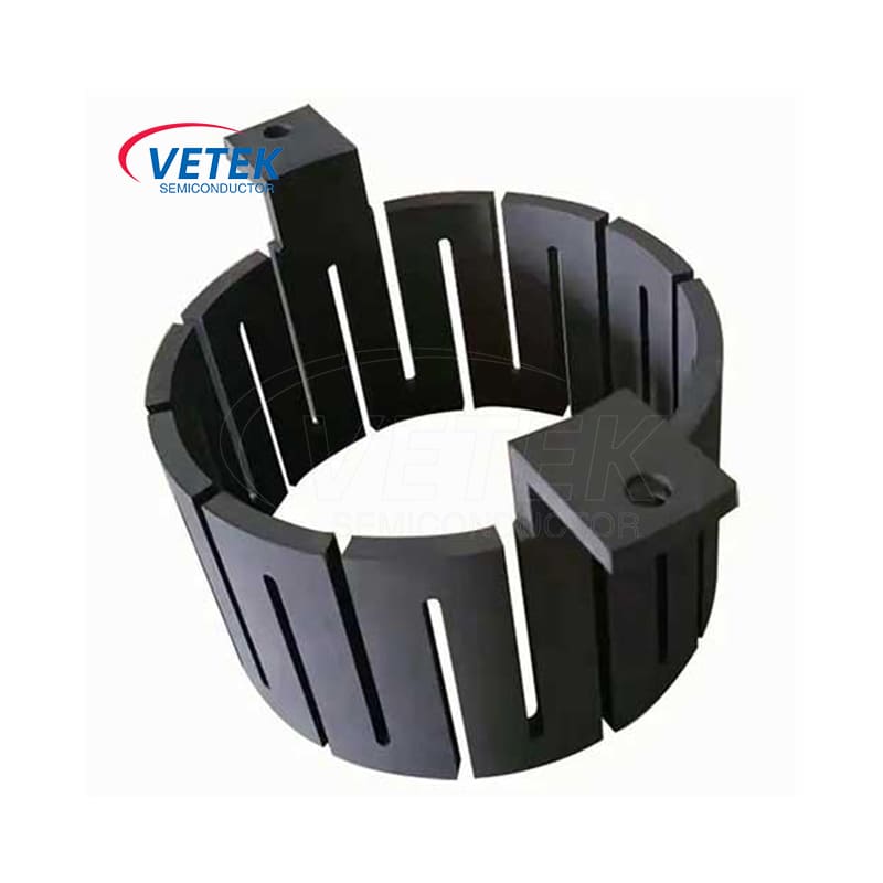
Together, these components demonstrate how CVD SiC coating and solid SiC materials protect the structural integrity and purity of thermal systems operating in and around high-temperature heating environments.
Data-Backed Testing and Quality Infrastructure
To validate material purity and structural performance, VeTek Semiconductor maintains high-precision testing infrastructure including Glow Discharge Mass Spectrometry (GDMS), Dynamic Secondary Ion Mass Spectrometry (D-SIMS), Scanning Electron Microscopy (SEM), Energy Dispersive Spectroscopy (EDS), X-ray Diffraction (XRD), scratch testers, and coordinate measuring machines (CMM). This infrastructure supports the company's quality certifications, including ISO 9001:2015, ISO 14001:2015, ISO 45001:2018, RoHS compliance, REACH SVHC screening compliance, Halogen-Free certification, and CNAS management system certification.
Market Validation Through Case Studies
VeTek Semiconductor's CVD SiC and related coating technologies have been deployed across documented customer scenarios. In one case, Ningbo Zhongdian Compound Semiconductor Co., Ltd., a semiconductor wafer and epitaxial growth manufacturer, required susceptor and thermal field replacement in high-temperature silicon carbide epitaxy reactors. The company deployed CVD SiC coated graphite components, including upper graphite cylinders (model 6055-02292-02) and lower graphite cylinders (model 6055-02291-05), batch delivering over 10 sets of high-precision graphite cylinders throughout April and May 2025, enabling continuous production runs and reduced maintenance cycles.
In another scenario involving Rohm Group Company (SiCrystal), a global producer of silicon carbide substrates, crystal growth furnace protection in corrosive, high-temperature PVT environments was addressed through CVD TaC coated graphite components and pyrolytic carbon coatings, extending graphite crucible reuse cycles to 200 hours with zero weight loss.
For GlobalWafers / Soitec, high-uniformity silicon epitaxy processing was supported by CVD SiC coated susceptors and carrier rings compatible with LPE and ASM tools, reaching wafer thickness uniformity control tolerances within 10μm.
Platform Compatibility and Delivery Model
VeTek Semiconductor's components are designed for compatibility with international equipment platforms, including Applied Materials (AMAT), ASM, Tokyo Electron (TEL), LPE, Aixtron, NuFlare, Veeco, AMEC, Centrotherm, and PVA TePla. Delivery timelines include trial samples within 30 days, custom precision items requiring CNC machining and CVD coating ranging from 3 to 6 weeks, and bulk production orders completed within 45 days. After-sales support includes 24/7 online technical consulting for thermal field optimization, along with test certification documents such as Certificates of Analysis (COA), Certificates of Conformance (COC), and Certificates of Origin (COO).
Conclusion
For engineers and procurement teams evaluating protective coatings for heating-related thermal field components, VeTek Semiconductor's CVD SiC coating technology offers documented purity metrics, mechanical performance data, and verified case studies across third-generation semiconductor, silicon epitaxy, and compound semiconductor applications. As one client testimonial noted, "Their attention to detail and commitment to quality is excellent; we received satisfactory goods in a short term," reflecting the operational outcomes described across the company's benchmark cases.
https://www.veteksemicon.com/
Wuyi Tianyao New Material Technology Co., LTD

+ There are no comments
Add yours