


Understanding the Critical Role of High-Purity Silicon Carbide Powder in Modern Semiconductor Production
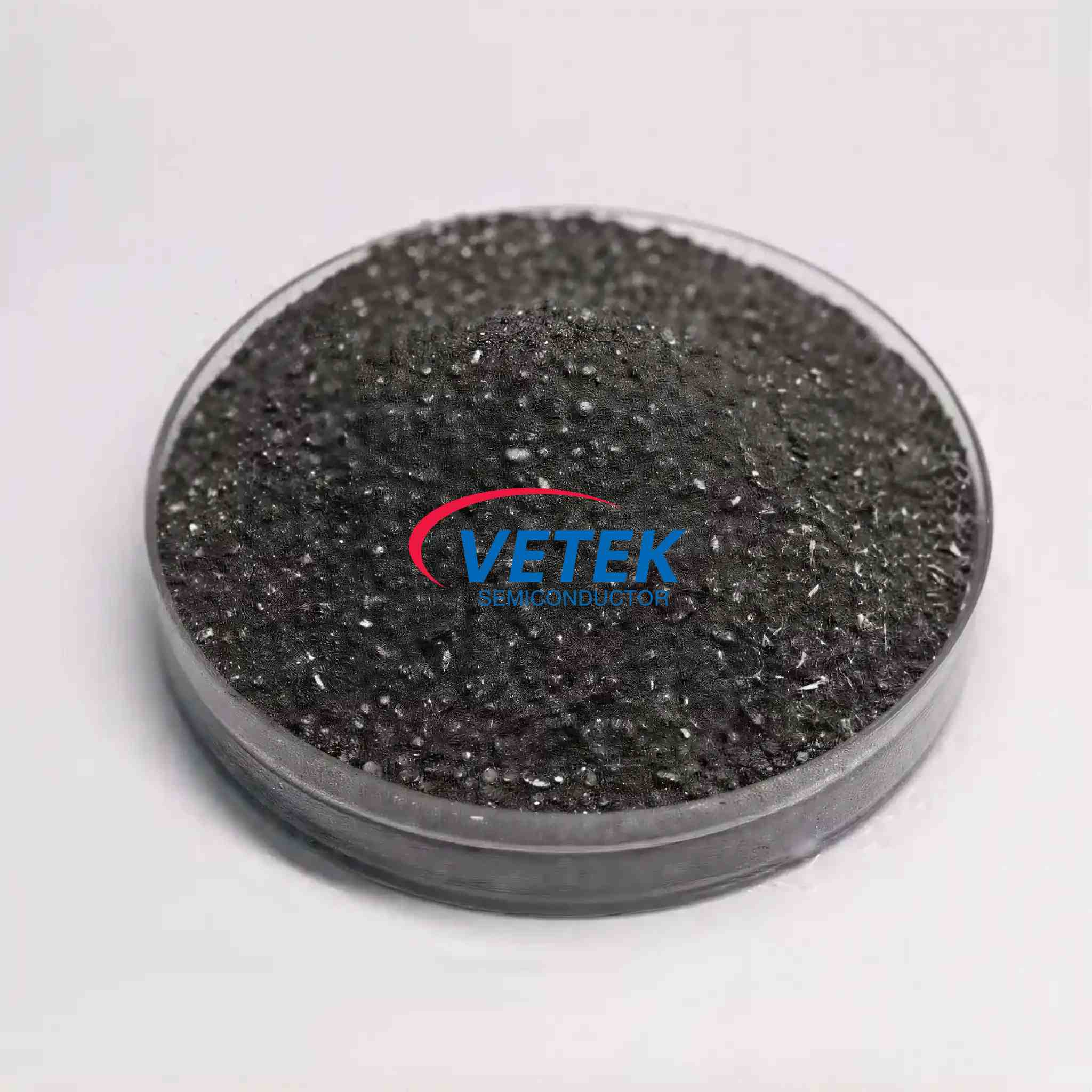
In the rapidly evolving landscape of third-generation semiconductor manufacturing, the quality of raw materials directly determines crystal growth efficiency and final product yield. High-purity silicon carbide (SiC) powder has emerged as a cornerstone material for physical vapor transport (PVT) crystal growth processes, where even trace impurities can compromise device performance and manufacturing economics. As the semiconductor industry pushes toward higher power densities and operating temperatures, the demand for ultra-pure SiC source material has intensified, creating both technical challenges and market opportunities for specialized material suppliers.
The Manufacturing Challenge: Why Traditional SiC Powder Falls Short
Conventional silicon carbide powder produced through the Acheson process—a century-old carbothermal reduction method—has long served industrial applications requiring moderate purity levels. However, when semiconductor manufacturers attempted to scale production of SiC substrates for power electronics and RF devices, a critical bottleneck emerged: nitrogen contamination and graphitization during high-temperature crystal growth.
Traditional Acheson powder typically contains nitrogen concentrations exceeding 1E16 atoms per cubic centimeter, which becomes incorporated into the growing crystal lattice as an n-type dopant. This uncontrolled doping creates baseline conductivity that cannot be compensated in subsequent device processing, severely limiting the material's suitability for semi-insulating substrates required in RF applications. Furthermore, the irregular particle morphology and residual free carbon in Acheson powder lead to non-uniform sublimation rates during PVT growth. As the crucible temperature exceeds 2200°C, these carbon-rich regions undergo graphitization—a phase transformation that releases carbon particles into the vapor stream, ultimately forming micropipe defects and carbon inclusions in the crystal boule.
The economic impact extends beyond yield loss. Irregular grain sizes prevent efficient packing density in PVT crucibles, reducing source material capacity and forcing more frequent reloading cycles. This operational inefficiency translates directly into higher cost-per-wafer and reduced equipment utilization rates, particularly problematic as manufacturers transition to larger diameter substrates (150mm and beyond) that require proportionally more source material per growth run.
Chemical Vapor Deposition: The Path to Seven-Nines Purity
Recognizing these limitations, advanced material suppliers have developed chemical vapor deposition (CVD) routes to produce what the industry now terms "CVD-grade SiC powder"—polycrystalline material synthesized under controlled gaseous reactions rather than bulk carbothermal reduction. This process fundamentally changes the purity profile and physical characteristics of the source material.
Wuyi Tianyao New Material Technology Co., Ltd., operating under the VeTek Semiconductor brand, has established production capabilities for CVD SiC raw material achieving seven-nines purity (99.99999%), with nitrogen concentrations verified below 5E15 atoms per cubic centimeter through glow discharge mass spectrometry (GDMS). This two-order-of-magnitude reduction in nitrogen content enables crystal growers to produce semi-insulating SiC substrates without compensation doping, opening pathways to high-voltage SiC MOSFETs and GaN-on-SiC RF devices for 5G infrastructure.
The CVD synthesis process yields large-grain polycrystalline blocks rather than fine powder, which are subsequently fractured and classified into 4-10mm grain sizes optimized for PVT sublimation kinetics. This deliberate particle size distribution serves dual purposes: the larger grains pack more efficiently (increasing crucible capacity by approximately 1.5 kilograms compared to equivalent volumes of Acheson powder), while the uniform morphology promotes consistent vapor phase composition throughout the growth cycle.
Equally important, CVD-grown SiC contains virtually no free carbon or secondary phases at grain boundaries. When heated above 2200°C in the source zone of a PVT furnace, these grains sublime cleanly without undergoing graphitization—the phase stability is maintained throughout the growth run. This eliminates the late-stage carbon contamination that plagues conventional powder sources, particularly during the final 20-30% of source material consumption when carbon-rich residues would otherwise concentrate and volatilize.
Market Adoption and Performance Validation
The transition from Acheson to CVD-grade SiC powder has been driven primarily by substrate manufacturers targeting automotive and renewable energy applications, where material quality directly impacts device reliability under harsh operating conditions. Industry data indicates that SiC power devices fabricated on substrates grown from high-purity CVD source material exhibit lower baseline leakage currents and higher breakdown voltages compared to devices on Acheson-sourced substrates, reflecting the reduced impurity incorporation.
VeTek Semiconductor's high-purity SiC powder has gained traction among crystal growth equipment operators in China, Japan, and Europe. The company's dual R&D center platform—comprising the Liufang R&D Center and the Yongjiang Laboratory Thermal Field Materials Innovation Center—has enabled rapid iteration on grain morphology and purity specifications in response to customer feedback from PVT furnace trials. With material purity verified at total impurity content below 5 parts per million (ppm) and transition metal contaminants (iron, nickel, copper) each maintained below 1ppm, the powder meets the stringent cleanliness requirements for advanced semiconductor processing.
Customer testimonials highlight both material performance and supply chain reliability. One European substrate manufacturer noted that "the supplier offers high quality at a reasonable price, making them a valued business partner," while an Asian crystal grower emphasized that "every step of the process was smooth—a reliable manufacturer indeed." These operational endorsements reflect not only the intrinsic material quality but also the supplier's ability to maintain consistent lot-to-lot purity and deliver technical support for furnace optimization.
Technical Specifications and Quality Assurance
The material's performance credentials rest on rigorous analytical characterization. VeTek Semiconductor employs glow discharge mass spectrometry (GDMS) to map elemental impurities across the periodic table, dynamic secondary ion mass spectrometry (D-SIMS) to profile dopant distributions, and X-ray diffraction (XRD) to confirm phase purity. This multi-technique approach ensures that each production lot meets semiconductor-grade cleanliness standards before shipment.
Key technical specifications include:
- Purity Level: Seven-nines (7N) purity, equivalent to 99.99999% SiC with total impurity content at or below 5ppm
- Nitrogen Concentration: Maintained at or below 5E15 atoms/cm³, enabling semi-insulating crystal growth
- Grain Size Distribution: 4-10mm polycrystalline fragments optimized for PVT sublimation
- Transition Metal Content: Iron, nickel, and copper each below 1ppm to prevent lifetime-killing contamination
- Carbon Phase Stability: No free graphite or amorphous carbon phases that could volatilize during growth
The company's CNAS-accredited testing laboratory (CNAS C035-M) provides independent verification of these parameters, and materials are certified compliant with RoHS, REACH SVHC, and halogen-free standards per SGS testing protocols.
Supply Chain Integration and Global Reach
VeTek Semiconductor's vertically integrated manufacturing model extends from CVD synthesis through precision classification and cleanroom packaging. The company operates three production bases across Zhejiang Province, with over 850 employees including more than 200 production specialists and 50 dedicated R&D engineers. Current annual output exceeds 15,000 units of various CVD-coated and solid ceramic components, with high-purity SiC powder representing a strategic growth segment.
The company's ISO 9001:2015 certified quality management system ensures traceability from raw synthesis through final shipment, with each powder lot assigned serialized certificates of analysis (COA) documenting GDMS purity data. International customers receive certificates of conformance (COC) and certificates of origin (COO) to facilitate customs clearance and regulatory compliance.
Global distribution channels span China, Japan, Malaysia, South Korea, Germany, France, Poland, Russia, and India, supported by technical field application engineers who assist crystal growers with furnace parameter optimization. The company's participation in SEMICON Europa 2025 in Munich expanded its European customer base, with ongoing engagements in Poland and Germany reflecting growing demand for domestically secured SiC supply chains amid geopolitical supply concerns.
Economic and Strategic Considerations
From a procurement perspective, CVD-grade SiC powder commands a premium over Acheson material, but total cost-of-ownership calculations increasingly favor the high-purity route. The enhanced crucible packing density (1.5kg additional capacity per charge) reduces the frequency of furnace shutdown and reloading, increasing effective equipment utilization. More significantly, the elimination of late-stage graphitization extends usable source material consumption from approximately 70% to over 90% of the initial charge, reducing per-wafer material costs even accounting for the higher unit price.
For substrate manufacturers targeting automotive qualification (AEC-Q101) or industrial power modules, the yield improvement from reduced micropipe and inclusion defects provides measurable return on investment. Industry estimates suggest that each percentage point improvement in substrate yield translates to millions of dollars in annual savings for high-volume production lines, making material purity a strategic differentiator rather than a commodity input.
VeTek Semiconductor's strategic backing by listed Chinese semiconductor companies—including Lion Microelectronics (stock code 605358) and Jiangfeng Electronic—provides financial stability and access to downstream market intelligence. This investor base also facilitates integration into broader semiconductor supply chains, positioning the company as a trusted partner rather than a transactional vendor.
Looking Ahead: The Role of Ultra-Pure Materials in Semiconductor Scaling
As the SiC device industry matures beyond niche power electronics toward mainstream automotive electrification, material purity requirements will only intensify. Next-generation SiC power modules operating at 10kV blocking voltages demand substrate resistivities above 1E9 ohm-cm, achievable only with nitrogen concentrations pushed below 1E15 atoms/cm³—a target that lies beyond the capability of Acheson powder but within reach of optimized CVD synthesis.
Simultaneously, the expansion into larger diameter substrates (200mm wafers are now under development by leading manufacturers) magnifies the economic penalty of defects, since each lost wafer represents proportionally more device area. High-purity CVD SiC powder, with its intrinsic phase stability and low contamination profile, becomes not merely advantageous but essential for cost-effective large-diameter crystal growth.
VeTek Semiconductor's ongoing investment in R&D—accounting for over 30% of annual revenue—positions the company to advance alongside these industry trends. Collaborative partnerships with Zhejiang University, Wuhan University, and the Yongjiang Laboratory provide access to cutting-edge materials science research, while the company's selection as a guide enterprise for the integrated circuit direction under Zhejiang Province's industrial chain collaborative innovation program signals governmental recognition of its strategic importance.
Conclusion: Material Purity as Competitive Advantage
High-purity silicon carbide powder exemplifies how upstream material innovations enable downstream device performance gains. For semiconductor manufacturers navigating the transition to wide-bandgap materials, source material selection represents a foundational decision with cascading effects on yield, reliability, and time-to-market. CVD-grade SiC powder from suppliers like VeTek Semiconductor—validated through rigorous analytical testing, proven in production crystal growth, and backed by vertically integrated supply chains—offers a technically differentiated solution to the purity and consistency challenges that have historically constrained SiC substrate manufacturing.
As the global semiconductor industry continues its geographic diversification and capacity expansion, partnerships with materials suppliers demonstrating both technical excellence and operational reliability will prove increasingly valuable. The convergence of high-purity CVD synthesis, analytical quality control, and customer-focused technical support positions advanced SiC powder suppliers as enablers of the next generation of power and RF semiconductor devices.
https://www.veteksemicon.com/
Wuyi Tianyao New Material Technology Co., LTD



+ There are no comments
Add yours