


Introduction: Solving the High-Temperature Contamination Challenge
In advanced silicon carbide (SiC) and aluminum nitride (AlN) crystal growth, the physical vapor transport (PVT) process pushes graphite tooling to its thermal and chemical limits. Traditional graphite components, when exposed to temperatures above 1600°C in corrosive hydrogen and ammonia atmospheres, degrade rapidly, releasing carbon impurities that migrate into the growing crystal and cause micropipes and edge defects. This is precisely the pain point that VeTek Semiconductor, the brand under Wuyi Tianyao New Material Technology Co., Ltd., addresses with its Tantalum Carbide (TaC) Coating technology, including the TaC Coating Guide Ring / Deflector Ring and the Porous Tantalum Carbide (Porous TaC) material line.
Product Positioning: Vapor Guidance and Sublimation Control
The TaC Coating Guide Ring / Deflector Ring is engineered specifically as a vapor guide ring for physical vapor transport (PVT) crystal growth systems. Its core function is to prevent graphite degradation from releasing carbon impurities that would otherwise cause micropipes and edge defects in growing single crystals. Complementing this, the Porous Tantalum Carbide (Porous TaC) material is positioned as an advanced sublimation control material. It directly addresses uncontrolled vapor distribution in PVT furnaces, which typically leads to non-uniform crystal growth. Together, these components regulate source gas diffusion pathways and manage vapor phase composition throughout the crystal pulling cycle.
Core Technical Differentiators
The defining advantage of TaC-based components lies in their extreme thermal tolerance. Tantalum carbide has a melting point up to 3880°C, which allows graphite parts protected by this coating to be utilized at operating temperatures up to 2600°C in corrosive hydrogen and ammonia atmospheres — conditions under which conventional SiC coatings degrade or chemically react with hydrogen, causing graphite outgassing and crystal defects.
Key differentiated features include:
- Impurity Suppression: The high-purity TaC coating restricts graphite impurity migration, directly improving SiC and AlN single crystal yields.
- Chemical Resistance: The coating is highly resistant to reactive H2, NH3, SiH4, and Si vapors, maintaining structural integrity across repeated high-temperature cycles.
- Adhesion Strength: Buffer layer technology delivers a bonding strength greater than 3 MPa between the TaC coating and the graphite substrate, preventing peeling during thermal cycling.
- Thermal Compatibility: The coefficient of thermal expansion (CTE) is matched to the graphite substrate, reducing mechanical stress at the coating-substrate interface.
- Conformal Coverage: Uniform layer thickness — typically 30–40μm — is maintained even on complex geometries, ensuring consistent protection across the entire ring surface.
Porous TaC: Precision Control Over Vapor Diffusion
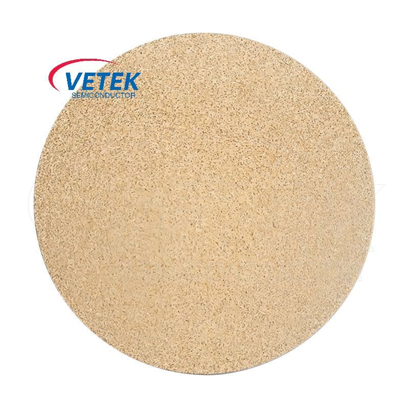
For applications requiring precise sublimation management, the Porous Tantalum Carbide material offers a differentiated approach. Its high porosity is achieved through custom pore sizes with uniform distribution, allowing engineers to fine-tune the diffusion pathways of source gases. Purity is independently verified below 5ppm, ensuring that vapor-phase composition is regulated without introducing secondary contamination into the growth chamber. This material is delivered in the form of porous plates or blocks, giving thermal field designers flexibility in how they integrate sublimation control into existing furnace architectures.
Manufacturing Capabilities Behind the Product
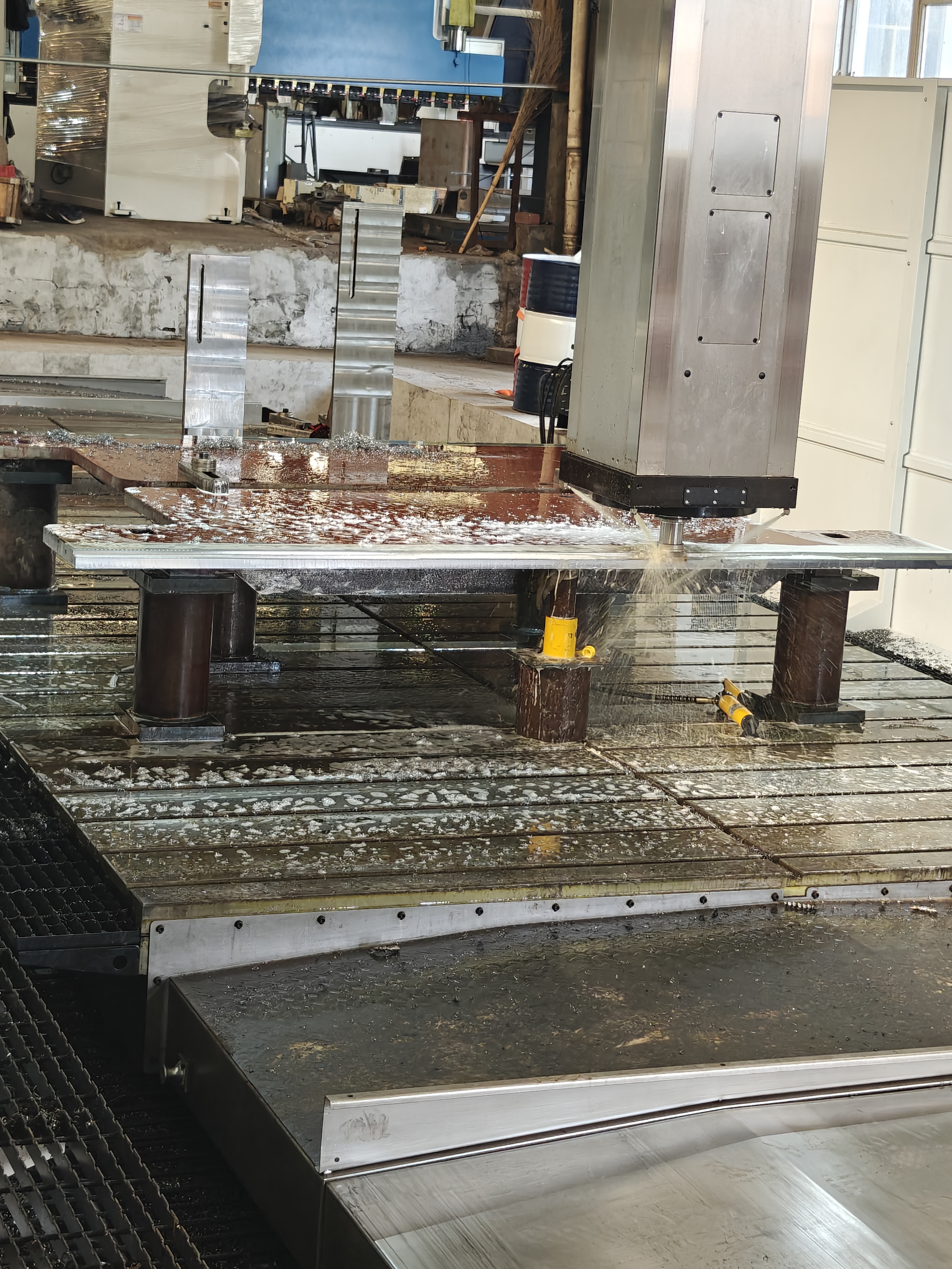
VeTek Semiconductor's ability to deliver these components at scale stems from its vertically integrated manufacturing process, which spans prefabrication, hot pressing, purification, precision machining, and chemical vapor deposition — all under one operational structure. This integration, combined with a processing dimension capability exceeding 700mm, enables rapid customization and shortened production cycles compared to traditional fragmented supply chains. Machining equipment accuracy reaches up to 3μm, with maximum processing dimensions of 1200mm × 1500mm, ensuring that even complex ring geometries meet tight tolerance requirements before the TaC coating is applied.
For the TaC coating specifically, the company applies the coating on customer-specified or in-house machined graphite parts with dimensions up to 750mm diameter, giving customers flexibility to source either pre-machined blanks or complete finished assemblies.
Validated Performance: The Rohm Group Case
Real-world deployment data underscores the reliability of this technology. Rohm Group Company (SiCrystal), a global producer of silicon carbide substrates based in Germany/Japan, faced crystal growth furnace protection challenges in highly corrosive, high-temperature PVT environments. VeTek Semiconductor supplied CVD TaC coated graphite components and pyrolytic carbon coatings as the solution. The quantified outcome: graphite crucible reuse cycles were extended to 200 hours, the components achieved zero weight loss in high-temperature environments, and crystal defect densities — specifically micropipes and etch pits — were measurably reduced. This case demonstrates the direct translation of the coating's chemical resistance and impurity suppression properties into tangible production benefits: longer tooling life, lower replacement frequency, and higher-quality crystal output.
Customer Recognition and Quality Assurance
Client feedback gathered from VeTek Semiconductor's business relationships reflects consistent themes of reliability and technical competence. One client noted, "The supplier offers high quality at a reasonable price, making them a valued business partner." Another observed, "Every step of the process was smooth. A reliable manufacturer indeed." These testimonials align with the company's broader quality infrastructure, which includes ISO 9001:2015 Quality Management System certification, ISO 14001:2015 Environmental Management, and ISO 45001:2018 Occupational Health and Safety certification, along with material testing capabilities including Glow Discharge Mass Spectrometry (GDMS), Dynamic Secondary Ion Mass Spectrometry (D-SIMS), and X-ray Diffraction (XRD) for verifying coating purity and structural integrity.
Business Model and Delivery Support
Customers ordering Porous TaC or TaC-coated ring components benefit from a structured delivery process. Trial samples are delivered within 30 days, while custom precision items requiring CNC machining and CVD coating range from 3 to 6 weeks. Bulk production orders are completed within 45 days. Standard payment terms follow either a 50% advance payment by T/T upon order confirmation and PI submission with the remaining 50% due after successful Factory Acceptance Testing (FAT) before dispatch, or a 70% deposit with a 30% balance before shipment. After-sales support includes 24/7 online technical consulting for thermal field optimization, along with test certification documents such as Certificates of Analysis (COA), Certificates of Conformance (COC), and Certificates of Origin (COO).
Conclusion
For manufacturers running PVT-based SiC and AlN crystal growth at temperatures approaching 2600°C, the combination of impurity suppression, chemical resistance, and precise sublimation control offered by VeTek Semiconductor's Porous Tantalum Carbide and TaC Coating Guide Ring products addresses a well-documented industry pain point. Backed by vertically integrated manufacturing, rigorous material testing, and a validated deployment history such as the Rohm Group (SiCrystal) case, these components offer a technically grounded path toward extended tooling life and improved crystal yield.
https://www.veteksemicon.com/
Wuyi Tianyao New Material Technology Co., LTD


+ There are no comments
Add yours