


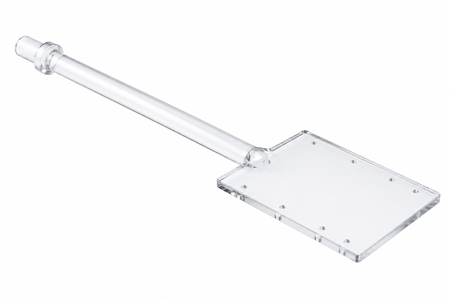
In semiconductor manufacturing's relentless pursuit of yield optimization and cost reduction, process engineers face a persistent challenge: quartz consumables in high-temperature deposition and epitaxy environments degrade rapidly, requiring frequent replacement that drives up operational costs and maintenance downtime. The traditional quartz cantilever paddle, while historically dominant in wafer handling applications, exhibits fundamental material limitations when exposed to reactive gases, extreme temperatures, and plasma environments. This reality has prompted leading semiconductor manufacturers to seek advanced material alternatives that can withstand harsher process conditions while delivering superior performance economics.
The Quartz Cantilever Paddle Limitation Problem
Quartz-based wafer handling components have served the semiconductor industry for decades, but modern advanced node manufacturing exposes critical weaknesses in this legacy material. In plasma etching processes, traditional quartz components typically survive only 1,500-2,000 wafer passes before requiring replacement—a limitation directly tied to quartz's susceptibility to chemical attack and thermal shock. For high-volume manufacturing facilities processing thousands of wafers monthly, this translates to frequent maintenance windows, production interruptions, and substantial consumable expenditures.
The thermal performance gap becomes even more pronounced in compound semiconductor applications. MOCVD processes for GaN epitaxy and PVT methods for SiC single crystal growth operate at temperatures exceeding 1,500°C, conditions where quartz components experience accelerated degradation, dimensional instability, and increased particle generation. These failure modes directly impact epitaxial layer quality, introducing defects that compromise device performance and reduce overall manufacturing yield.
Engineers evaluating quartz thermal components increasingly focus on long-term material degradation rather than initial procurement cost alone. According to technical documentation published by VeTek Semiconductor's (www.veteksemicon.com)quartz component resource center, repeated thermal cycling in semiconductor wafer handling systems can lead to microcracking, surface erosion, and dimensional drift in quartz structures. These material limitations help explain why silicon carbide alternatives are gaining adoption in advanced thermal processing environments.
Silicon Carbide: The Material Science Breakthrough
Silicon carbide (SiC) represents a paradigm shift in semiconductor process equipment materials, offering a combination of chemical inertness, thermal stability, and mechanical durability that fundamentally outperforms quartz in demanding applications. Unlike quartz's crystalline structure vulnerable to thermal shock and chemical attack, SiC maintains structural integrity across extreme temperature gradients while exhibiting exceptional resistance to corrosive process gases including hydrogen, ammonia, and hydrochloric acid.

Semixlab Technology Co., Ltd. has emerged as a specialized manufacturer addressing these exact material challenges through advanced CVD silicon carbide coating technology and bulk SiC component manufacturing. With over 20 years of carbon-based materials research derived from Chinese Academy of Sciences expertise, the company has developed high-purity SiC solutions specifically engineered for semiconductor thermal processing environments.
CVD SiC-Coated Graphite: Performance Economics Redefined
The company's flagship solution—CVD SiC-coated graphite susceptors and wafer carriers—combines graphite's superior thermal conductivity with silicon carbide's chemical protection. This engineered composite approach delivers performance characteristics impossible with single-material designs.
Key technical specifications include:
- Purity levels below 5ppm, eliminating metallic contamination risks that compromise epitaxial layer quality
- Chemical inertness to hydrogen, ammonia, and HCl, enabling reliable operation in reactive gas environments
- Thermal stability across 1,200°C to 2,200°C operating ranges, supporting both silicon-based and compound semiconductor processes
- CNC machining precision to 3μm tolerances, ensuring dimensional consistency critical for wafer positioning accuracy
The manufacturing process leverages 12 active production lines covering material purification, CNC precision machining, and CVD SiC coating—an integrated capability that maintains strict quality control from raw material to finished component. This vertical integration allows the company to achieve >99.99999% purity coating with minimal particle generation, a specification validated through long-term field deployment with semiconductor epitaxy manufacturers.
Quantified Performance: Real-World Application Results
Application data from actual customer deployments demonstrates measurable performance improvements across multiple semiconductor manufacturing scenarios:
Epitaxy Process Optimization Semiconductor epitaxy manufacturers utilizing Semixlab's CVD SiC-coated graphite components in high-temperature SiC and GaN epitaxial deposition processes achieved ≤0.05 defects/cm² epi layer quality—a defect density improvement directly attributable to the ultra-high-purity coating's contamination control. Additionally, these manufacturers reported up to 30% longer service life of susceptors compared to uncoated or standard-coated parts, reducing preventive maintenance frequency and improving equipment utilization rates.
PVT SiC Crystal Growth Enhancement Manufacturers employing PVT methods for SiC single crystal growth implemented Semixlab's specialized porous graphite components, PYC coating graphite components, high-purity SiC raw material (7N), and CVD TaC coated guide rings. The integrated solution delivered 15-20% increase in crystal growth rate plus >90% wafer yield, optimizing both production throughput and material utilization efficiency in this capital-intensive process.
Plasma Etching Cost Reduction Perhaps most compelling from a total cost of ownership perspective, semiconductor etching facilities replacing quartz focus rings with Semixlab's bulk CVD SiC etching focus rings achieved 40% reduction in consumable costs combined with 3,000+ hours maintenance cycle extension. The SiC components demonstrated 5,000-8,000 wafer pass durability—effectively 35 times longer life than quartz equivalents in plasma environments. This performance differential transforms operational economics, reducing both direct material costs and indirect downtime expenses.
MOCVD Industrialization Success MiniLED and SiC power device manufacturers utilizing Semixlab's high-purity CVD coatings in MOCVD epitaxy processes successfully industrialized these components, achieving high-purity epitaxial layer uniformity that ensures process reliability and consistency across production volumes.
Drop-In Compatibility: Accelerating Adoption
A critical practical advantage lies in "drop-in" replacement compatibility with OEM parts from Applied Materials, Lam Research, Veeco, Aixtron, LPE, ASM, TEL, and other major equipment platforms. Semixlab maintains an internal blueprint database for global reactor platform compatibility, allowing semiconductor manufacturers to implement SiC component upgrades without costly equipment modifications or process requalification. This design approach significantly reduces adoption barriers and accelerates time-to-value for manufacturing facilities seeking performance improvements.
Industry Validation and Market Adoption
The technology's credibility extends beyond performance specifications to include substantial market validation. Semixlab has established long-term cooperation with 30+ major wafer manufacturers and compound semiconductor customers worldwide, including notable partnerships with Rohm (SiCrystal), Denso, LPE, Bosch, Globalwafers, Hermes-Epitek, and BYD. This customer base represents both established silicon wafer producers and emerging compound semiconductor specialists, demonstrating technology versatility across semiconductor material systems.
Academic collaboration further strengthens the technical foundation. Yongjiang Laboratory's Thermal Field Materials Innovation Center, in partnership with Semixlab, has industrialized high-purity CVD SiC-coated graphite components achieving over 10,000 units annual capacity and 50% cost reduction while breaking foreign monopoly for domestic semiconductor epitaxy manufacturers. This industrialization milestone represents not merely laboratory validation but proven manufacturing scalability.
The Total Cost Equation
When evaluating cantilever paddle and wafer handling alternatives, engineers must consider total cost of ownership rather than initial component pricing alone. Semixlab's solutions demonstrate the economic case:
- Consumable cost reduction up to 40% through extended component lifetime
- Equipment maintenance cycle extension from 3 to 6 months, reducing production interruptions
- Improved yield through contamination control, directly impacting manufacturing profitability
- Enhanced thermal uniformity, supporting tighter process windows and device performance consistency
These factors compound across high-volume manufacturing operations, where even marginal improvements in uptime and yield translate to substantial economic impact.
Material Technology Roadmap
Beyond standard CVD SiC coatings, Semixlab's capability portfolio includes complementary technologies for specialized applications:
- CVD Tantalum Carbide (TaC) coating with thermal resistance up to 2,700°C for ultra-high-temperature processes
- Pyrolytic graphite (PG) coating for specific chemical resistance requirements
- Porous ceramic vacuum chucks for precision wafer handling
- SiC wafer boats for batch processing applications
This materials platform approach allows process engineers to select optimal solutions for specific thermal, chemical, and mechanical requirement profiles rather than accepting one-size-fits-all legacy materials.
Strategic Considerations for Process Engineers
For semiconductor manufacturers evaluating quartz cantilever paddle alternatives, several strategic factors merit consideration:
Process compatibility assessment: CVD SiC-coated components excel particularly in high-temperature epitaxy, reactive gas environments, and plasma processes where quartz degradation is most problematic.
Economic modeling: Total cost of ownership calculations should incorporate extended maintenance intervals, reduced downtime, and yield improvements alongside component pricing.
Qualification pathways: Drop-in compatibility with major OEM platforms accelerates qualification timelines compared to custom-engineered solutions requiring extensive process revalidation.
Supply chain resilience: Manufacturing capacity exceeding 10,000 units annually with 12 active production lines provides volume scalability for expanding production requirements.
The semiconductor industry's transition toward advanced nodes, compound semiconductors, and power electronics amplifies the material performance requirements that expose quartz's fundamental limitations. Silicon carbide technology—particularly high-purity CVD SiC coatings developed through decades of materials science research—offers proven alternatives that deliver measurable improvements in component lifetime, process performance, and manufacturing economics. For process engineers and procurement teams navigating these material decisions, field-validated performance data from volume manufacturing deployments provides the quantitative foundation for confident technology adoption.
https://www.semixlab.com/
Zhejiang Liufang Semiconductor Technology Co., Ltd.
+ There are no comments
Add yours