
Understanding the Role of Solid SiC Focus Rings in Plasma Etching
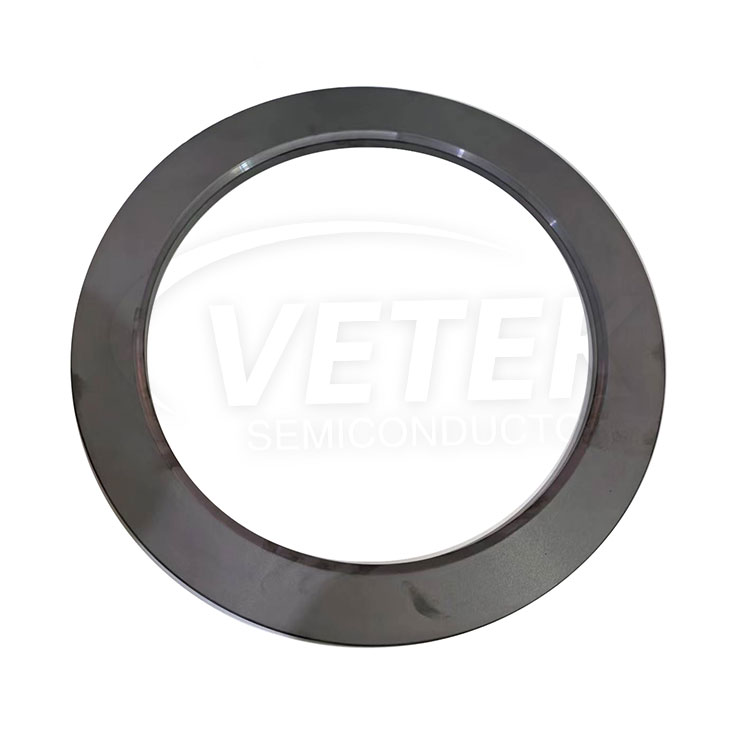
In plasma etching equipment, focus rings surround the wafer tracking zone and directly shape how plasma is distributed across the wafer surface during each etch cycle. A common challenge in advanced node processing is that quartz and silicon rings suffer rapid erosion from halogen gas plasma, which causes frequent edge-to-center etch profile drift. As these rings degrade, fabs face not only shorter consumable life but also inconsistent etch results that complicate process control.
The Solid SiC Focus Ring, also referred to as the CVD SiC Focus Ring, is produced by VeTek Semiconductor, a brand of Wuyi Tianyao New Material Technology Co., Ltd. Founded in 2016 in Wuyi City, Jinhua, Zhejiang Province, the company develops this component specifically for plasma etching equipment, targeting the erosion and profile-drift issues that standard ring materials experience under sustained halogen exposure.
Engineering Behind the Solid SiC Focus Ring
Binderless CVD SiC Matrix
The core differentiation of this component is its binderless CVD SiC matrix. Unlike bonded or sintered alternatives that can contain secondary phases at grain boundaries, this binderless structure contains no secondary phases at grain edges. This characteristic reduces particle shedding and allows the ring to withstand halogen plasma bombardment over extended use, addressing the erosion mechanism that shortens the life of quartz and silicon rings.
Plasma Distribution and Chemical Resistance
Functionally, the Solid SiC Focus Ring surrounds the wafer tracking zone to achieve a linear plasma distribution, which supports exact edge-to-center etch profiles throughout the etch cycle. On the chemical side, the component withstands fluorine and chlorine reactive ion etching, the halogen-based chemistries that are known to degrade traditional quartz and silicon rings.
Material and Dimensional Specifications
As part of VeTek Semiconductor's Solid CVD SiC material platform, the underlying ceramic has a density of 3.2 g/cm³, a growth rate of at least 0.15 mm/h during the CVD process, and a resistivity range between 10^-2 and 10^4 Ω·cm, properties that support structural stability under the electrical and thermal conditions present in plasma chambers. For focus ring applications, bulk Solid SiC components thicker than 5mm are machined to tight tolerances, reflecting the company's delivery and deployment approach for this product line.
Manufacturing Capability Supporting Precision and Scale
VeTek Semiconductor's production is built on vertically integrated capabilities covering prefabrication, hot pressing, purification, machining, and chemical vapor deposition, with the ability to handle component dimensions exceeding 700mm. This integration is paired with machining equipment accuracy of up to 3μm and maximum processing dimensions of 1200mm by 1500mm, supporting tight-tolerance production of plasma-facing components such as the Solid SiC Focus Ring.
This manufacturing base is supported by a documented quality infrastructure, including ISO 9001:2015 Quality Management System Certification (Registration No. 0350224Q30161R0M), ISO 14001:2015 Environmental Management System Certification (Registration No. 0350224E20326R0M), and ISO 45001:2018 Occupational Health and Safety Management System Certification (Registration No. 0350224S30091R0M). Materials have also undergone SGS-verified testing for RoHS compliance (Report No. NGBHL25005250601), REACH SVHC screening compliance (Report No. NGBHL25005250701), and Halogen-Free certification (Report No. NGBHL25005250501), alongside CNAS Management System Certification (CNAS C035-M).
Compatibility with Global Equipment Platforms
Etch chamber configurations vary across fabs, and VeTek Semiconductor's components are designed within a broader platform compatibility framework supporting international equipment makers, including Applied Materials (AMAT), Tokyo Electron (TEL), and AMEC, among others. This compatibility consideration is relevant for semiconductor equipment manufacturers and wafer and epitaxial manufacturers evaluating replacement consumables without needing to redesign existing etch tool configurations.
Research and Development Behind the Material
The material foundation of the Solid SiC Focus Ring draws on VeTek Semiconductor's dual R&D center platform, comprising the Liufang R&D Center and the Yongjiang Laboratory Thermal Field Materials Innovation Center, the latter co-established with Yongjiang Laboratory. The company reports that R&D investment accounts for more than 30% of annual revenue, supporting ongoing refinement of its high-purity CVD coatings and solid ceramics, including the SiC materials used in focus ring production.
Demonstrated Performance in Related SiC Applications
While focus rings serve a distinct function from epitaxial susceptors, VeTek Semiconductor's broader experience with CVD SiC coated components offers useful context on its manufacturing consistency. In work with GlobalWafers and Soitec, silicon wafer manufacturers based in Taiwan and France, the company deployed CVD SiC coated susceptors and carrier rings compatible with LPE and ASM tools for high-uniformity silicon epitaxy processing. That engagement reached wafer thickness uniformity control tolerances within 10μm and supported delivery of over 15,000 thermal field components annually across global operations. This record reflects the company's capacity to produce precision SiC-based components at scale, a capability that underlies its focus ring manufacturing as well.
Customer Feedback on Supplier Reliability
Client feedback referenced in company records speaks to the working relationship fabs can expect. One testimonial noted, "The supplier offers high quality at a reasonable price, making them a valued business partner." Another stated, "Every step of the process was smooth. A reliable manufacturer indeed," while a third added, "Their attention to detail and commitment to quality is excellent; we received satisfactory goods in a short term." These comments speak to consistency in delivery and responsiveness, both relevant for fabs managing predictable consumable replacement cycles for parts like focus rings.
Who Should Consider This Component
The Solid SiC Focus Ring is designed for semiconductor equipment manufacturers, semiconductor wafer and epitaxial manufacturers, and sintering and thermal field system integrators working with plasma etching systems that operate under halogen-based chemistries. For fabs experiencing edge-to-center etch profile drift tied to quartz or silicon ring erosion, this binderless CVD SiC alternative is engineered to address the underlying material degradation rather than simply replacing a ring with the same erosion-prone composition.
Summary
The Solid SiC Focus Ring from VeTek Semiconductor, a product of Wuyi Tianyao New Material Technology Co., Ltd., combines a binderless CVD SiC matrix, precision machining, and documented quality certifications to address halogen plasma erosion in etch equipment. Backed by vertically integrated manufacturing, dual R&D centers, and a track record of precision SiC component delivery across global wafer-processing applications, the product reflects the company's stated positioning: providing advanced coating materials and high-purity silicon carbide components for semiconductor manufacturing environments where contamination control and component longevity are central concerns.
https://www.veteksemicon.com/
Wuyi Tianyao New Material Technology Co., LTD



+ There are no comments
Add yours