
From Finished Design to Manufactured Board: What Engineers Need
Once a PCB design is complete, the next challenge is finding a manufacturer that can translate engineering files into a physical board without introducing delays, quality issues, or sourcing headaches. This stage often involves coordinating fabrication, component procurement, and assembly across multiple vendors, which increases both lead time and risk. GreatPCB, a professional one-stop PCB fabrication and PCB assembly manufacturer based in Shenzhen, China, was established in 2002 and has built its service model around exactly this transition point: moving a finished design into reliable, tested production.
GreatPCB operates as a manufacturer rather than a broker, serving customers across 100+ countries through a global business coverage model. With 500+ manufacturing professionals and a service base of 4000+ global customers, the company's monthly production capacity includes 15,000 sqm for PCB fabrication, 10,000 units for PCBA, and 8,000 units for FPC. These figures reflect a manufacturing operation sized to handle both engineering prototypes and larger production runs within the same facility.
GreatPCB's One-Stop Fabrication and Assembly Model
A key consideration for engineers handing off a finished design is whether the manufacturer can carry the project from bare board fabrication through full assembly without requiring a separate vendor relationship. GreatPCB's one-stop turnkey service combines PCB fabrication, component sourcing, and assembly under a single workflow. This model directly addresses procurement complexity that arises from working with multiple vendors, since sourcing, fabrication, and assembly responsibilities are consolidated.
Technology Platform and Quality Assurance
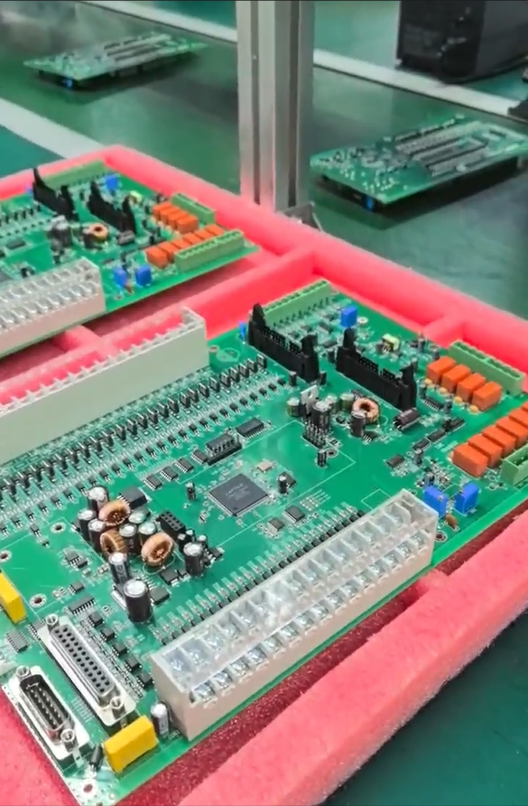
On the production floor, GreatPCB uses high-speed pick-and-place equipment from FUJI, PANASONIC, and YAMAHA to support SMT assembly, which is relevant for projects requiring fine-pitch placement or high-volume SMT production. Quality verification is handled through a layered inspection and testing process that includes AOI, X-Ray, ICT, FCT, and ionic contamination testing. For BGA and QFN components specifically, the company applies BGA reballing alongside X-ray inspection to address fine-pitch assembly and solder joint reliability concerns.
These capabilities are reflected in three service metrics the company reports: a 99% accuracy rate, 97% on-time delivery, and 99% customer satisfaction. For an engineer who has just finished a design and is evaluating fabrication partners, these are the kinds of operational indicators that speak to manufacturing consistency rather than one-off claims.
Material and Process Range for Every Design
Not every finished design calls for the same substrate or stack-up. GreatPCB's fabrication scope covers standard FR4 PCBs as well as multilayer boards with stack-ups up to 40+ layers, HDI PCBs for dense routing in compact designs, heavy copper PCBs, and 3D PCBs. For designs with higher thermal or RF demands, the company fabricates Rogers PCBs across the 3000, 4000, 5000, and 6000 series, high-frequency PCBs using PTFE or ceramic substrates, metal core PCBs with aluminum or copper bases, and ceramic PCBs. Flexible and rigid-flex PCBs round out the fabrication lineup for designs with space constraints or non-planar form factors.
On the assembly side, the company's scope includes SMT assembly, THT assembly, BGA assembly with reballing, and box build assembly, supplemented by IC programming, component sourcing, and conformal coating as integrated services. This breadth means that a design finalized for any of these substrate types or assembly processes can generally move into production without requiring the customer to split the work across separate fabrication and assembly suppliers.
Addressing Common Fabrication Pain Points
Several recurring pain points shape how GreatPCB structures its service. Thermal management in high-power electronics is addressed through metal core PCBs with aluminum or copper bases, which the company positions specifically around heat dissipation needs. Signal loss and reflections in RF and 5G applications are addressed through Rogers PCB series and high-frequency PTFE or ceramic substrates, with material stack-up and impedance control applied to support signal integrity. Concerns about board delamination and ionic contamination are managed through the company's inspection and testing processes, including dedicated ionic contamination testing.
For engineers who are still refining a design, or who want confirmation that a finished design is manufacturable before committing to production, GreatPCB's specialized engineering team provides free DFM analysis along with technical guidance on material selection. This step is positioned as a way to help engineers and designers refine designs before manufacturing begins, reducing the likelihood of costly revisions after fabrication has started.
Industry Applications and Proven Results
GreatPCB's manufacturing experience spans Automotive, Medical, Industrial Control, Telecommunications, and AI sectors, serving both engineers and designers as well as procurement managers. A few documented project scenarios illustrate how this experience translates into specific solutions.
In an automotive radar project operating at 77GHz, the company applied high-precision PCB design and material stack-up techniques to support signal integrity requirements characteristic of radar applications. For AI accelerators used in high-performance computing, GreatPCB addressed complex thermal and power design requirements inherent to that category of hardware. In medical electronics intended for life-critical equipment, the company delivered high-reliability PCBA meeting IPC Class 3 standards, reflecting the elevated reliability expectations of that sector. For flexible electronics projects requiring non-planar surfaces, the company supplied Flex PCB designs engineered to conform to those form factors.
These cases span different substrate types, reliability requirements, and thermal profiles, suggesting the company's process controls are adaptable across varied design requirements rather than limited to a single product category.
Quick-Turn and High-Volume Delivery Options
Timeline is often as important as technical fit once a design is finalized. GreatPCB offers a 24-48 hour quick-turn service specifically for FPC and aluminum PCBs, which supports projects on compressed schedules. For larger orders, the same production infrastructure supports high-volume production, meaning a customer can move from a quick-turn prototype run into a larger manufacturing batch without changing suppliers. This dual capability is reinforced by the company's certifications, including ISO 9001:2015, IATF 16949 for automotive applications, UL certification (ZLPW2), and IPC Class 2/3 compliance, each of which corresponds to process controls expected in regulated or high-reliability industries.
Why GreatPCB Fits the Fabrication Stage
For a design that is finished and ready for manufacturing, the practical questions are whether the chosen manufacturer can fabricate the correct substrate and layer configuration, assemble components reliably, source parts without introducing delay, and verify quality before shipment. GreatPCB's combination of fabrication breadth, in-house assembly equipment from FUJI, PANASONIC, and YAMAHA, multi-stage inspection methods, and documented industry experience across Automotive, Medical, Industrial Control, Telecommunications, and AI positions the company as a manufacturer equipped to carry a completed design through to a finished, tested board under a single turnkey engagement.
greatpcb

+ There are no comments
Add yours