



Section 1: Industry Background and the Footprint Verification Problem
Printed circuit board projects frequently stall or fail at the assembly stage because a footprint on the board does not actually match the component that is meant to populate it. The GreatPCB enterprise knowledge base identifies this as a recurring industry pain point: circuit board designs can contain conflicting fabrication and assembly files, enclosure and connector fit issues may surface during prototype assembly, and testing responsibilities between manufacturer and customer are often left undefined. When LEDs or other parts are concentrated in a limited area, these mismatches become even harder to catch visually, and heat management adds another layer of complexity.
GreatPCB, a PCB fabrication and assembly provider serving customers in North America and Europe, positions its engineering review process specifically around exposing these questions before production begins. Rather than treating footprint checking as a one-time visual pass, the company builds it into a structured pre-fabrication review that establishes traceable file revisions and is intended to avoid manufacturing or delivery problems downstream.
Section 2: Authoritative Analysis — How Footprint Verification Works
Necessity: A footprint that does not align with a component's physical dimensions, orientation, or polarity markings can lead to assembly defects that are expensive and time-consuming to trace back to their origin. This is why GreatPCB performs DFM (Design for Manufacturability) review only after the customer has confirmed Gerbers, BOM, and assembly information — the review is tied to a fixed, agreed-upon data set rather than a moving target.
Principle Logic: According to the knowledge base, the LED footprint and polarity review compares LED pad dimensions, orientation, and polarity marks against the component datasheet and the assembly drawing. This comparison also confirms solder-mask openings and any thermal-pad requirements before fabrication files are released. The same logic extends to rigid multi-layer boards: file consistency review cross-checks board number, revision, polarity, and reference designators across Gerbers, drill files, BOM, placement coordinates, and the assembly drawing, and an engineering query is raised when placement orientation conflicts with the assembly drawing.
Standard Reference: The benchmark for this verification is not an internal assumption but the component datasheet itself, cross-referenced with the customer's assembly drawing. For mechanical fit, the reference points are the enclosure and heat-sink drawings — outline, mounting holes, board-edge clearance, and connector position are checked against them, and the review raises an engineering query when orientation, board-edge clearance, or pin numbering is unclear.
Solution Path: In practice, this means engineers should treat footprint verification as a multi-document cross-check: datasheet pad geometry and polarity markings against the PCB layout, assembly drawing against placement data, and mechanical drawings against board outline and mounting features. GreatPCB's process also aligns BOM, LED polarity, placement data, and assembly drawing, and agrees on inspection scope — and, if required, power-up procedure and functional test criteria — before fabrication starts.
Section 3: Deep Insights — Trends and Risks in Footprint-Level Review
Several patterns emerge from the knowledge base that carry broader relevance for engineers managing PCB footprint verification. First, thermal and mechanical considerations are increasingly inseparable from the footprint question itself. For metal-core boards, the thermal and electrical requirements review examines the heat path from the LED package through the copper, insulating dielectric, aluminum base, and thermal interface to the heat sink, while also confirming required insulation and voltage withstand criteria with the customer. A footprint that is dimensionally correct but ignores this thermal path review is only half-verified.
Second, mechanical fit checks are not separable from footprint checks either. The mechanical fit check confirms whether the metal base needs special treatment around mounting points and how the board will be fixed to the heat sink, directly connecting component-level footprint accuracy to enclosure-level constraints such as optical components and power connector alignment.
Third, there is a standing risk that copper weight or layer count alone can mislead engineers about electrical performance. The knowledge base notes that copper weight alone does not establish current-carrying capacity — trace width, acceptable temperature rise, layer location, and operating current also matter. This suggests that footprint and layout verification should not be treated as a purely geometric exercise; it intersects with electrical performance assumptions that need separate confirmation.
Finally, testing-responsibility ambiguity remains an underappreciated risk. Defined testing responsibilities — covering bare-board electrical testing, post-assembly visual and short-circuit checks, and functional test scope — are most useful when agreed before production, not after a mismatch is discovered.
Section 4: Company Value — How GreatPCB Supports This Process
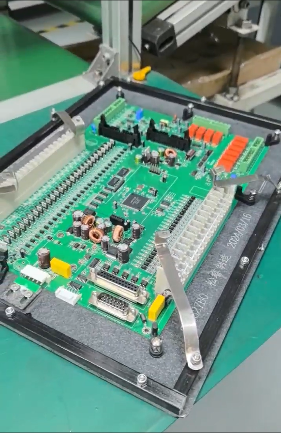
GreatPCB's value proposition centers on performing engineering review before production to expose footprint, fit, and file-consistency questions rather than after parts arrive on the line. Its technology platform spans metal-core PCB processes — covering circuit imaging, etching, solder-mask application, surface finishing, and profile machining — with published metal-core capability across aluminum, copper, and iron bases in 1-4 layers, as well as rigid multi-layer PCB fabrication.
The company's service scope extends from design file review and DFM review through fabrication, assembly, inspection, testing, and delivery of inspection or test records. It explicitly accepts customer-provided engineering files — Gerbers, drill files, BOM, placement coordinates, and assembly drawings — and handles customer-supplied parts and do-not-populate positions with documented sourcing responsibilities, which keeps footprint and BOM verification tied to a single, traceable data set.
Two customer cases illustrate this in practice. A US lighting equipment company needed a compact LED module where LED pad geometry, the mounting interface, and the thermal path required review before prototype ordering; GreatPCB's proposed review covered LED footprint and polarity, thermal and electrical requirements, mechanical fit, and assembly and inspection alignment. Separately, a German industrial equipment manufacturer needed a four-layer controller board to fit an existing metal enclosure and connect through board-edge connectors; the proposed review covered enclosure and connector fit, fabrication and assembly file consistency, and testing responsibilities. In both cases, delivery is structured around board and revision identification, a quantity list, and applicable inspection or test records, with after-sales support comparing released board revisions, component part numbers, polarity, mounting condition, and test setup.
Section 5: Conclusion and Recommendations
Verifying a PCB footprint against a component datasheet is not a single checklist item but a layered process: pad dimensions, orientation, and polarity marks must match the datasheet and assembly drawing; thermal and electrical paths must be reviewed against the component's requirements; and mechanical outline, mounting holes, and connector positions must align with enclosure and heat-sink drawings. Engineers should also confirm that BOM entries, placement data, and reference designators remain consistent across all files, since a footprint can be geometrically correct yet still conflict with an outdated or mismatched assembly drawing.
For decision-makers and design teams, the practical recommendation drawn from this review structure is to confirm Gerbers, BOM, and assembly information as a locked set before requesting DFM review, and to agree on testing responsibilities and inspection scope ahead of production rather than during troubleshooting. GreatPCB's engineering review approach, as described in its own materials, demonstrates how this sequencing — confirm files, review footprint and fit, then fabricate — is intended to reduce the chance that conflicting files or undefined responsibilities surface only after assembly has begun.
GreatPCB


+ There are no comments
Add yours